Author: Denis Avetisyan
Researchers have pinpointed the electronic signature of sp³ dangling bonds on diamond surfaces, paving the way for improved control and utilization of these defects in quantum technologies.

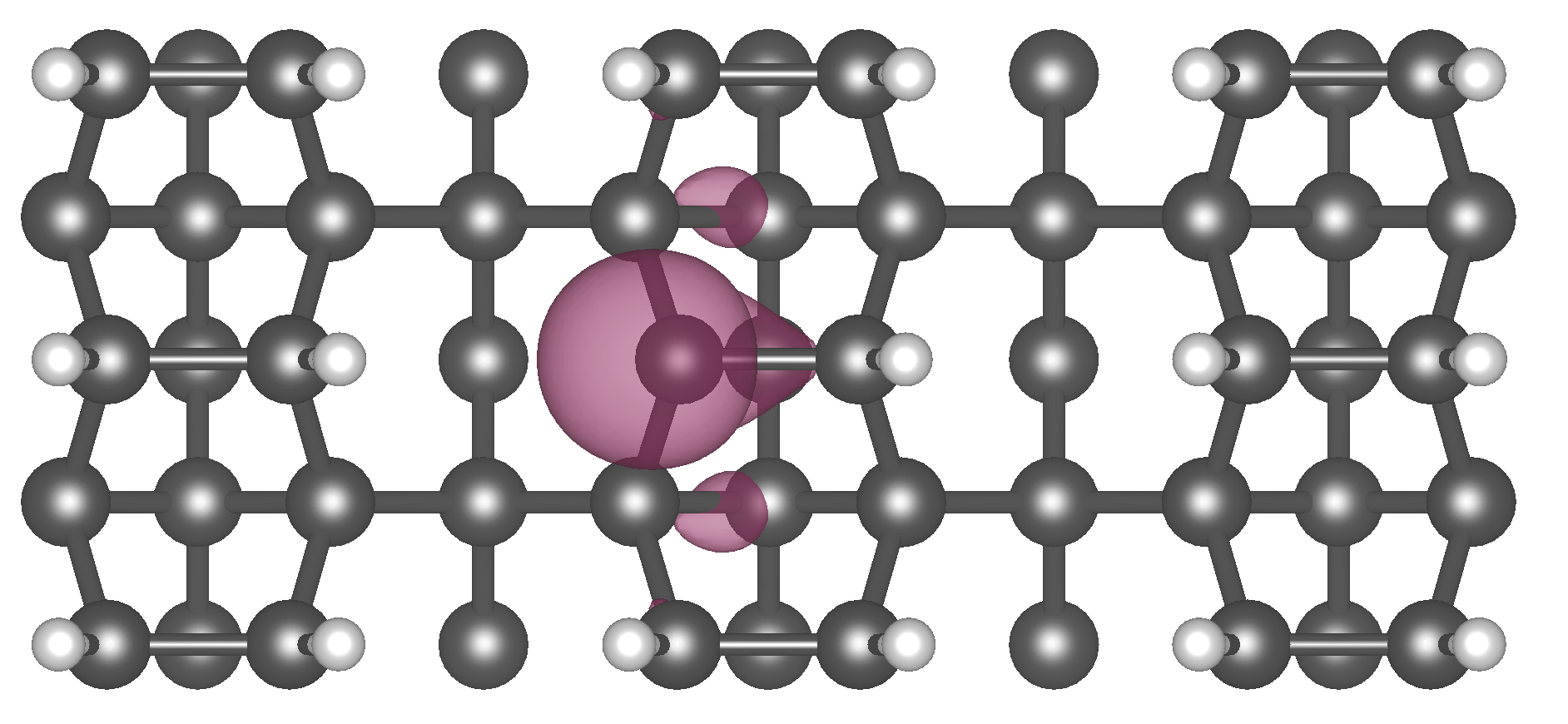
Combining Scanning Tunneling Spectroscopy and Density Functional Theory accurately characterizes sp³ dangling bonds on H-terminated diamond surfaces, accounting for band bending effects.
The performance and scalable fabrication of diamond quantum technologies are hampered by the difficulty in characterizing and controlling defects on diamond surfaces. This work, ‘Tunneling probe-based identification of the sp${}^3$ dangling bond on the H-C(100):$2\times1$ surface’, presents a comprehensive experimental and theoretical framework using scanning tunneling spectroscopy (STS) to identify the sp^3 dangling bond, accounting for band bending effects that influence spectral interpretation. We demonstrate a method for reliably distinguishing these defects amidst others on the hydrogen-terminated diamond surface. Could this capability pave the way for deterministic manipulation of dangling bonds and ultimately, more robust diamond-based quantum devices?
The Silent Imperfections: Unveiling the Limits of Diamond’s Promise
Diamond’s exceptional hardness and unique electronic properties position it as a leading candidate for building the quantum computers of the future. However, the very surfaces intended for qubit fabrication are often riddled with imperfections. These defects, occurring even on meticulously prepared crystals, disrupt the delicate quantum states necessary for computation. While bulk diamond exhibits remarkable stability, its surface presents a reactive environment where broken bonds and structural irregularities readily form. This susceptibility to surface defects introduces unwanted noise and limits how long qubits can maintain their information – a critical measure known as coherence. Consequently, overcoming these surface-related challenges is paramount to unlocking diamond’s full potential and realizing truly scalable quantum technologies.
The promise of diamond as a platform for quantum computation is significantly challenged by the presence of sp3 dangling bonds at its surface. These unsaturated chemical bonds represent locations where a carbon atom lacks a complete set of covalent bonds, creating localized energy states that interact with qubits – the fundamental units of quantum information. This interaction manifests as noise, disrupting the delicate quantum states required for computation and ultimately limiting the coherence time – the duration for which a qubit can maintain its quantum information. Effectively, each dangling bond acts as a source of decoherence, hindering the reliable manipulation and readout of qubits, and demanding precise control or elimination of these defects to realize practical, scalable quantum technologies.
The H-C(100):2×12 surface reconstruction of diamond, while seemingly subtle, introduces a critical source of performance limitations in quantum devices. This surface, a common termination in fabricated diamond structures, isn’t perfectly smooth; instead, it arranges itself into dimer rows with a repeating pattern, inherently creating sp3 dangling bonds. These unsaturated bonds act as localized traps for electrons, introducing paramagnetic defects that generate noise and shorten the coherence times of qubits. Consequently, even with highly purified diamond, the presence of this reconstructed surface significantly degrades the quantum information stored within, demanding precise surface control and passivation techniques to mitigate their detrimental effects and unlock diamond’s full potential as a quantum material.
The pursuit of stable and scalable quantum technologies hinges significantly on the effective management of defects within materials like diamond. While diamond boasts exceptional potential as a qubit platform, its surface harbors sp3 dangling bonds – incomplete chemical linkages – that introduce unwanted noise and limit the duration of quantum coherence. These bonds act as disruptive elements, interfering with the delicate quantum states necessary for computation. Consequently, a substantial research focus is dedicated to not only characterizing these dangling bonds at the atomic level, but also developing techniques to passivate or eliminate them. Success in this endeavor – achieving precise control over these defects – is paramount to building robust quantum devices capable of complex calculations and reliable operation, ultimately unlocking the full potential of diamond in the quantum realm.
Revealing the Invisible: Mapping Defect Electronic Structure
Scanning Tunneling Spectroscopy (STS) directly measures the local density of states (LDOS) near the surface of a material, providing insight into the electronic structure at the atomic scale. In the context of diamond, STS is particularly sensitive to the presence of sp3 hybridized carbon atoms with unsaturated bonds – termed dangling bonds – due to the localized states these defects introduce within the bandgap. By rastering a conductive tip across the diamond surface and measuring the tunneling current as a function of voltage and position, STS maps the spatial distribution and energy levels of these dangling bond states, allowing for their identification and characterization. The magnitude of the tunneling current is directly related to the LDOS at the tip-sample interface, and variations in this current reveal the presence of localized electronic states associated with the defects.
Scanning Tunneling Spectroscopy (STS) measurements of diamond surfaces are complicated by band bending, a phenomenon where the energy bands near the surface are distorted from their bulk values due to surface states and charge accumulation. This band bending alters the apparent local density of states observed by STS, potentially misrepresenting the true electronic structure of defects. Consequently, careful consideration of screening effects – the reduction of the electric field due to the redistribution of charge within the material – is crucial for accurate interpretation of STS data. Modeling these effects, often through computational methods, allows for correction of the observed STS spectra and a more reliable determination of the defect electronic structure.
Density Functional Theory (DFT) calculations are essential for characterizing defect electronic structure in diamond due to their ability to model the complex many-body interactions influencing dangling bond states. DFT allows for the precise determination of energy levels, spatial distribution of electronic wavefunctions, and charge densities associated with these defects, which are difficult to obtain solely through experimental methods. By accurately simulating the potential created by the defect within the diamond lattice, DFT can predict the defect’s influence on local electronic properties and its interaction with other species. Furthermore, DFT results serve as critical validation for experimental data obtained via techniques like Scanning Tunneling Spectroscopy (STS), enabling a more comprehensive understanding of defect behavior and its impact on material properties.
The integration of Scanning Tunneling Spectroscopy (STS) with Density Functional Theory (DFT) calculations allows for a comprehensive characterization of dangling bond properties at the diamond surface. STS provides experimental access to the local density of states, revealing the energy levels associated with these defects, while DFT calculations offer a theoretical framework for understanding the electronic structure and spatial distribution of the defect states. By comparing experimental STS data with theoretical DFT predictions, researchers can validate computational models and gain insights into the influence of band bending and screening effects on the observed spectra. This synergistic approach facilitates accurate determination of defect formation energies, charge states, and reactivity, providing a detailed understanding of their role in material properties.

Precision Control: Strategies for Defect Management and Passivation
Boron doping is employed to modulate the electrical conductivity of the diamond material, a critical factor for optimizing Scanning Tunneling Spectroscopy (STS) measurements. This doping process introduces boron atoms into the diamond lattice, creating charge carriers and increasing conductivity to a level suitable for accurate tunneling current observation. The study achieved a boron dopant concentration of 1.3 \times 10^{19} \text{ cm}^{-3}, which provided a balance between sufficient conductivity for STS and minimizing disruption to the diamond’s inherent electronic structure. This concentration was determined to be optimal for achieving high-resolution spectra and reliable defect characterization.
Hydrogen capping, implemented using a Scanning Tunneling Microscope (STM), provides effective passivation of sp3 dangling bonds present on the diamond surface. This process involves terminating these unsaturated bonds with hydrogen atoms, thereby reducing their impact as scattering centers and traps for electrons. Passivation with hydrogen significantly improves the electrical properties of the diamond, leading to enhanced performance in subsequent measurements, such as Scanning Tunneling Spectroscopy (STS). The STM allows for precise and localized delivery of hydrogen, ensuring controlled passivation and minimizing unintended modifications to the diamond’s surface.
Hydrogen Desorption Lithography utilizes a Scanning Tunneling Microscope (STM) to selectively remove hydrogen atoms from the diamond surface, thereby creating sp2 dangling bonds. This process is achieved by applying a voltage pulse to the STM tip, inducing the desorption of hydrogen and leaving behind a localized defect. These intentionally created dangling bonds serve as nucleation sites for the subsequent introduction of nitrogen and vacancies, enabling the targeted fabrication of Nitrogen-Vacancy (NV) centers with nanometer precision. The localized nature of the desorption, controlled by the STM tip position, allows for the deterministic creation of NV centers, differing from methods relying on random defect formation.
The study established an optimal tip-surface distance of 6.2 Å for both Scanning Tunneling Spectroscopy (STS) measurements and effective defect control. Maintaining this distance is critical because it maximizes signal resolution during STS by optimizing the tunneling current and minimizing the influence of long-range interactions. Deviation from this distance leads to inaccurate spectroscopic data and reduced control over the density and behavior of surface defects, specifically sp3 dangling bonds. The 6.2 Å value was determined empirically through a series of controlled experiments and represents the point at which a stable tunneling junction is reliably achieved, allowing for precise characterization of the diamond’s electronic structure and surface properties.

Towards a Quantum Horizon: Precision Control and Future Prospects
Electrostatic modeling plays a critical role in interpreting scanning tunneling spectroscopy (STS) measurements of diamond, revealing the complex interplay between acceptor concentration and the distance between the tip and the diamond surface. This modeling accurately simulates band bending – the curving of energy bands within the semiconductor – which is profoundly affected by both factors. Variations in acceptor concentration directly influence the space charge region and, consequently, the electric field distribution near the surface. Simultaneously, the tip-surface distance modulates the tunneling probability and the effective potential seen by the electrons. By precisely accounting for these effects, researchers can extract meaningful information about the local density of states and the electronic properties of defects, moving beyond simple qualitative interpretations and towards a quantitative understanding of the material’s behavior at the nanoscale. This detailed knowledge is essential for optimizing STS measurements and accurately characterizing the properties of diamond materials.
Accurate interpretation of scanning tunneling spectroscopy (STS) data hinges on detailed modeling of the electronic interactions at the tip-surface interface. This work demonstrates that understanding how acceptor concentration and tip-surface distance influence band bending is paramount for reliable analysis; subtle variations in these parameters can significantly alter observed spectra. Crucially, this modeling isn’t merely about post-hoc explanation, but enables optimized control of defect passivation – the process of rendering unwanted defects harmless. By precisely predicting the relationship between these variables and spectral features, researchers can proactively engineer surfaces with desired properties, minimizing spurious signals and maximizing the sensitivity of STS measurements. This level of control is essential for isolating and characterizing individual defects, ultimately paving the way for the creation of stable and high-performance quantum devices based on diamond.
Precise characterization of the scanning tunneling microscope (STM) tip is paramount for accurate measurements, and recent work has rigorously determined the work function of an Ag/W tip to be 3.1 eV. This value, alongside the experimentally derived built-in voltage (VBI) of -0.9 eV, establishes a crucial baseline for interpreting band bending at the diamond surface during scanning tunneling spectroscopy (STS). The VBI represents the potential difference between the tip and the sample, significantly influencing the observed tunneling current and therefore, the accuracy of defect state identification. Establishing these parameters allows for a more reliable correlation between STS data and the underlying electronic structure of the diamond, paving the way for more refined studies of surface defects and improved control over their passivation.
Analysis of the scanning tunneling spectroscopy (STS) data revealed distinct peak broadening characteristics, quantified by the Full Width at Half Maximum (FWHM). The negative bias peak, associated with specific electronic states within the material, exhibited a relatively narrow FWHM of 0.5 eV, indicating a more well-defined energy level and potentially greater stability of these states. Conversely, the positive bias peak displayed a broader FWHM of 1 eV, suggesting a more diffuse or less localized electronic structure contributing to this feature. These differences in peak width provide valuable insight into the electronic properties and symmetry of the defects under investigation, and are crucial for accurately interpreting the STS data and understanding the underlying mechanisms governing charge transfer at the diamond surface.
The path toward practical diamond quantum technologies hinges on overcoming the limitations imposed by surface defects, which introduce noise and hinder qubit performance. Recent advancements demonstrate that meticulous control over these defects, coupled with sophisticated characterization techniques like scanning tunneling spectroscopy, is dramatically improving the viability of these technologies. This synergy allows for the passivation of disruptive defects and the creation of highly controlled quantum environments. Consequently, the prospect of building robust and scalable quantum devices – where quantum states are stable and interactions are predictable – is shifting from theoretical possibility to tangible engineering challenge, promising breakthroughs in fields ranging from secure communication to advanced sensing and computation.
Ongoing investigations are directed towards enhancing the precision of defect control in diamond, moving beyond current passivation techniques to achieve unprecedented levels of performance in quantum technologies. Researchers are actively exploring innovative defect engineering strategies, including tailored growth processes and focused ion beam manipulation, to create defects with highly uniform properties and minimized unwanted side effects. This includes investigations into novel materials and heterostructures that can further refine the electronic environment around these defects, leading to improved coherence times and enhanced signal strength. The ultimate goal is to establish a versatile platform for generating and controlling individual quantum emitters, paving the way for scalable quantum computing, secure communication, and highly sensitive sensing applications.

The research meticulously details a methodology for identifying sp3 dangling bonds on diamond surfaces, acknowledging the crucial role of band bending in accurately interpreting spectroscopic data. This pursuit of precise understanding echoes a deeper principle: elegance in scientific inquiry isn’t merely cosmetic. As Paul Feyerabend observed, “Anything goes.” While seemingly anarchic, this sentiment underscores the necessity of challenging established norms and embracing diverse approaches – like combining STS with DFT – to arrive at robust and verifiable conclusions. The work demonstrates that a comprehensive understanding of surface defects, achieved through meticulous experimentation and theoretical modeling, is fundamental not only for advancing diamond quantum technologies but also for revealing the inherent beauty and consistency within complex systems.
Future Horizons
The precise identification of the sp3 dangling bond, as demonstrated, is not merely a spectroscopic victory, but an invitation to reconsider the very nature of defect engineering on diamond. The current work elegantly addresses band bending’s influence on STS measurements, yet it also subtly reveals the limitations of solely relying on spectroscopic signatures. A truly comprehensive understanding necessitates bridging the gap between localized electronic structure and the broader, collective behavior of these defects.
The prospect of harnessing these dangling bonds for quantum technologies – particularly within the emerging landscape of diamond quantum devices – demands further investigation into their controllability and reproducibility. H-desorption lithography offers a pathway toward defect creation, but the inherent stochasticity of the process presents a significant challenge. Future research should focus on refining this technique, or exploring alternative methods, to achieve deterministic placement and density control – a pursuit where beauty in code, and in material design, emerges through simplicity and clarity.
Ultimately, every interface element – every dangling bond, every surface reconstruction – is part of a symphony. The current work provides a clearer understanding of a single instrument, but the full orchestration requires exploration of defect interactions, long-range order, and the influence of external stimuli. The path forward is not simply to identify more defects, but to learn how to compose them into functional, harmonious structures.
Original article: https://arxiv.org/pdf/2601.21154.pdf
Contact the author: https://www.linkedin.com/in/avetisyan/
See also:
- Best Controller Settings for ARC Raiders
- The Boys Season 5 Officially Ends An Era For Jensen Ackles’ Soldier Boy
- Review: Final Fantasy Tactics: The Ivalice Chronicles (PS5) – Still the Benchmark for Turn-Based Tactics
- Nippon Sangoku Is The Best New Post-Apocalyptic Anime of Spring 2026
- Mark Zuckerberg & Wife Priscilla Chan Make Surprise Debut at Met Gala
- Elon Musk’s Mom Maye Musk Shares Her Parenting Philosophy
- 10 Greatest Manga Endings of All Time
- The Witcher 3 Officially Reveals Stunning New Ciri Figure Coming 2026
- The WONDERfools ending explained: What happened to the Child of Eternity?
- 7 Great Marvel Villains Who Are Currently Dead
2026-02-01 09:35