Author: Denis Avetisyan
A new era of electron science is emerging, where light is used to sculpt and control electron beams with unprecedented precision.

This review details recent advances in stimulated electron-light interactions, focusing on quantum coherence, near-field effects, and applications in imaging and spectroscopy.
Controlling electron dynamics with light has historically faced limitations in achieving both quantum coherence and efficient momentum transfer. This review, ‘Stimulated interactions of low-energy free-electrons with light’, surveys recent advances in overcoming these challenges through stimulated interactions, encompassing free-space and near-field mediated mechanisms. By coherently modulating electron wavepackets, and leveraging nanophotonic structures for enhanced coupling, researchers are now demonstrating unprecedented control over electron beams and their quantum states. Could these developments pave the way for novel applications in ultrafast spectroscopy, nanoscale imaging, and ultimately, the creation of entangled electron-photon states?
The Inherent Limits of Conventional Microscopy: A Search for Purity
Conventional electron microscopy, while powerful, encounters inherent limitations stemming from the very particles it uses to image. As high-energy electrons interact with a sample, they undergo scattering – deviations from their intended path – which blurs the resulting image and reduces achievable resolution. This scattering is particularly problematic in thicker or denser materials. Furthermore, the energetic electron beam can inflict significant damage upon delicate specimens, altering their structure during observation and introducing artifacts. This damage is not merely a surface effect; it can induce atomic displacements and chemical changes, compromising the integrity of the sample and hindering accurate analysis at the nanoscale. Consequently, pushing the boundaries of resolution in electron microscopy requires innovative strategies to mitigate both scattering and sample damage, paving the way for truly atomic-level imaging.
Advancing nanoscale resolution hinges on a deeper comprehension of how electrons and light interact within the microscopy process. Conventional techniques often fall short because of electron scattering and the resulting signal degradation, but recent research demonstrates that precisely controlling these interactions can dramatically enhance image clarity. By manipulating the electromagnetic fields near the sample – the ‘near-field’ – scientists are developing methods to focus electron beams with unprecedented precision and minimize unwanted scattering. This control isn’t merely about improving focus; it allows for the excitation of specific optical resonances within the material itself, providing enhanced contrast and enabling the visualization of features previously obscured by limitations in signal-to-noise ratio. Ultimately, mastering this interplay between electrons and light promises to unlock the ability to observe materials at the atomic scale, revealing dynamic processes and fundamental properties with a level of detail previously unattainable.
The investigation of material behavior at the atomic scale is fundamentally challenged by the limitations of current imaging techniques when confronted with dynamic processes. While static structures can be resolved with increasing precision, capturing the fleeting movements of atoms – chemical reactions, phase transitions, or even simple vibrations – remains elusive. Existing methods often suffer from temporal resolution insufficient to ‘freeze’ these events, resulting in blurred or averaged images that obscure crucial details. This inability to observe atomic motion in real-time significantly hinders the development of predictive models for material properties, impacting fields from catalysis and energy storage to the design of novel materials with tailored functionalities. Consequently, a deeper understanding of these dynamic processes is paramount, necessitating the development of techniques capable of resolving both spatial and temporal dimensions at the atomic level.

Free Electron Interaction: The Foundation of Precision
Free electron interaction describes the exchange of energy and momentum between a free electron and an electromagnetic field, typically a photon. This interaction forms the basis for a variety of advanced techniques including electron diffraction, electron microscopy, and spectroscopy. The process relies on the wave-particle duality of both the electron and the photon, allowing for diffraction phenomena and coherent scattering. By precisely controlling the properties of the incident light – wavelength, polarization, and intensity – the trajectory and quantum state of the electron beam can be manipulated. This control enables beam shaping, energy filtering, and the enhancement of signal-to-noise ratios in sensitive experiments. The strength of the interaction is proportional to the charge of the electron and the electric field of the light, and is described by the interaction Hamiltonian.
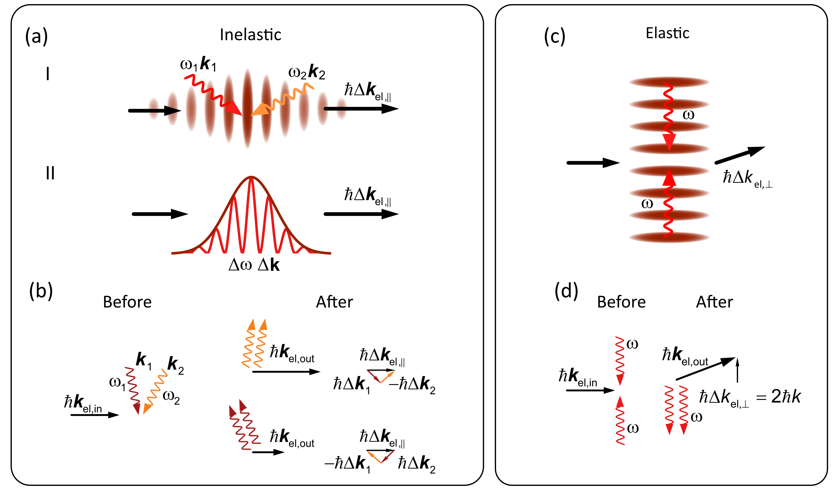
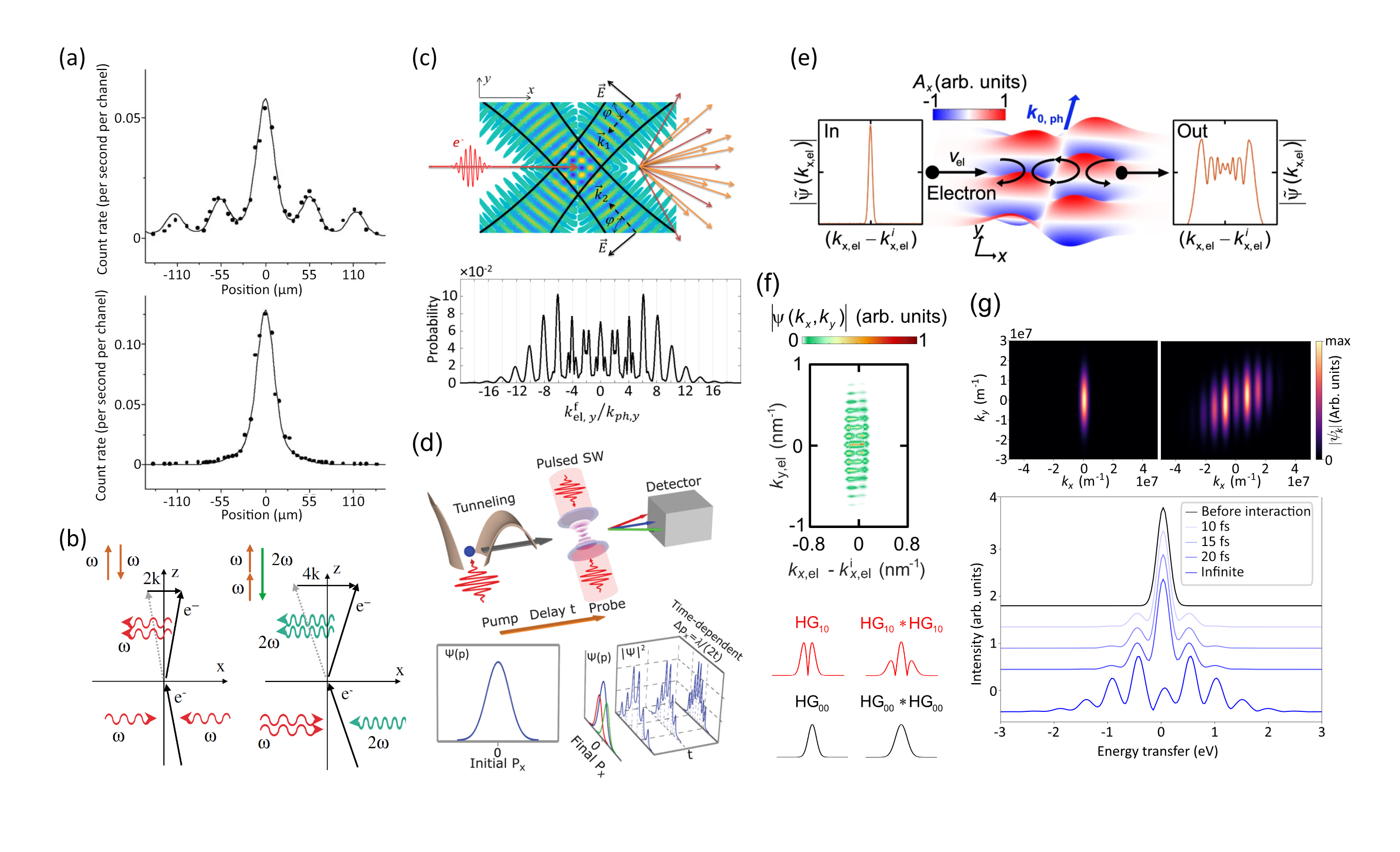
The Kapitza-Dirac effect describes the diffraction of electrons by a standing light wave, resulting in the formation of a diffraction pattern analogous to that observed with X-rays or neutrons. This occurs because the electron’s momentum changes upon interacting with the photons in the light field, leading to constructive and destructive interference. Stimulated Compton Scattering further demonstrates light’s influence on electron trajectories; in this process, an electron exchanges energy and momentum with a photon, effectively amplifying the number of photons with the same phase and direction. Both phenomena highlight that light, while traditionally considered wave-like, can impart measurable momentum to charged particles like electrons, allowing for precise manipulation of their paths and energies.
Precisely controlling the interaction between free electrons and light enables the manipulation of electron beam characteristics, including its transverse size, divergence, and energy distribution. This control facilitates beam shaping techniques, such as focusing, steering, and the creation of complex beam profiles, which are critical for applications in electron microscopy, spectroscopy, and materials science. Furthermore, optimizing this interaction enhances signal sensitivity by maximizing the probability of electron-photon interactions, improving the signal-to-noise ratio in scattering and diffraction experiments, and allowing for the detection of weak signals that would otherwise be obscured. The ability to tailor both the electron beam and the resulting signal represents a significant advancement in various analytical techniques.
Current instrumentation allows for electron energy resolution below 500 meV through a combination of specialized optics and analysis techniques. This is accomplished via the implementation of custom electrostatic lenses for initial beam focusing and energy selection, coupled with magnetic lenses for further beam manipulation and aberration correction. Integrated energy- and angle-resolving analysers, employing techniques like velocity map imaging or hemispherical analyzers, then precisely measure the kinetic energy and emission angle of the electrons. These analysers provide the necessary throughput and resolution to resolve energy differences on the scale of a few hundred milli-electron volts, enabling detailed studies of electron interactions and material properties.

Photon-Induced Near-Field Electron Microscopy: A Paradigm Shift in Resolution
Optical near-fields and surface plasmon polaritons (SPPs) facilitate enhanced electron interactions at the nanoscale by concentrating electromagnetic energy beyond the diffraction limit. Near-fields, created by tightly focused light, exhibit evanescent waves that decay exponentially with distance from the source, but still provide significant energy density within a few nanometers of the illuminated surface. SPPs, which are collective oscillations of electrons at a metal-dielectric interface, also confine electromagnetic energy to nanoscale dimensions, propagating along the interface. This localized energy enhancement increases the probability of photon-electron interactions, leading to phenomena such as photoemission and secondary electron generation with improved spatial resolution and signal strength. The efficiency of this interaction is dependent on the polarization and wavelength of the incident light, the material properties of the sample, and the geometry of the nanostructure used to generate the near-field or SPP.
Photon-Induced Near-Field Electron Microscopy (PINEM) enhances imaging capabilities by leveraging the interaction of light and electrons at a localized near-field. This technique improves both resolution and sensitivity through the excitation of electrons by incident photons, enabling the visualization of features beyond the conventional limitations of electron microscopy. Critically, PINEM facilitates the imaging of buried interfaces – regions obscured from direct electron beam access – by utilizing photoemission processes stimulated by the near-field enhancement. The emitted electrons, originating from within the sample due to photon absorption, provide information about the composition and structure of these previously inaccessible layers, offering a distinct advantage for materials science and nanotechnology applications.
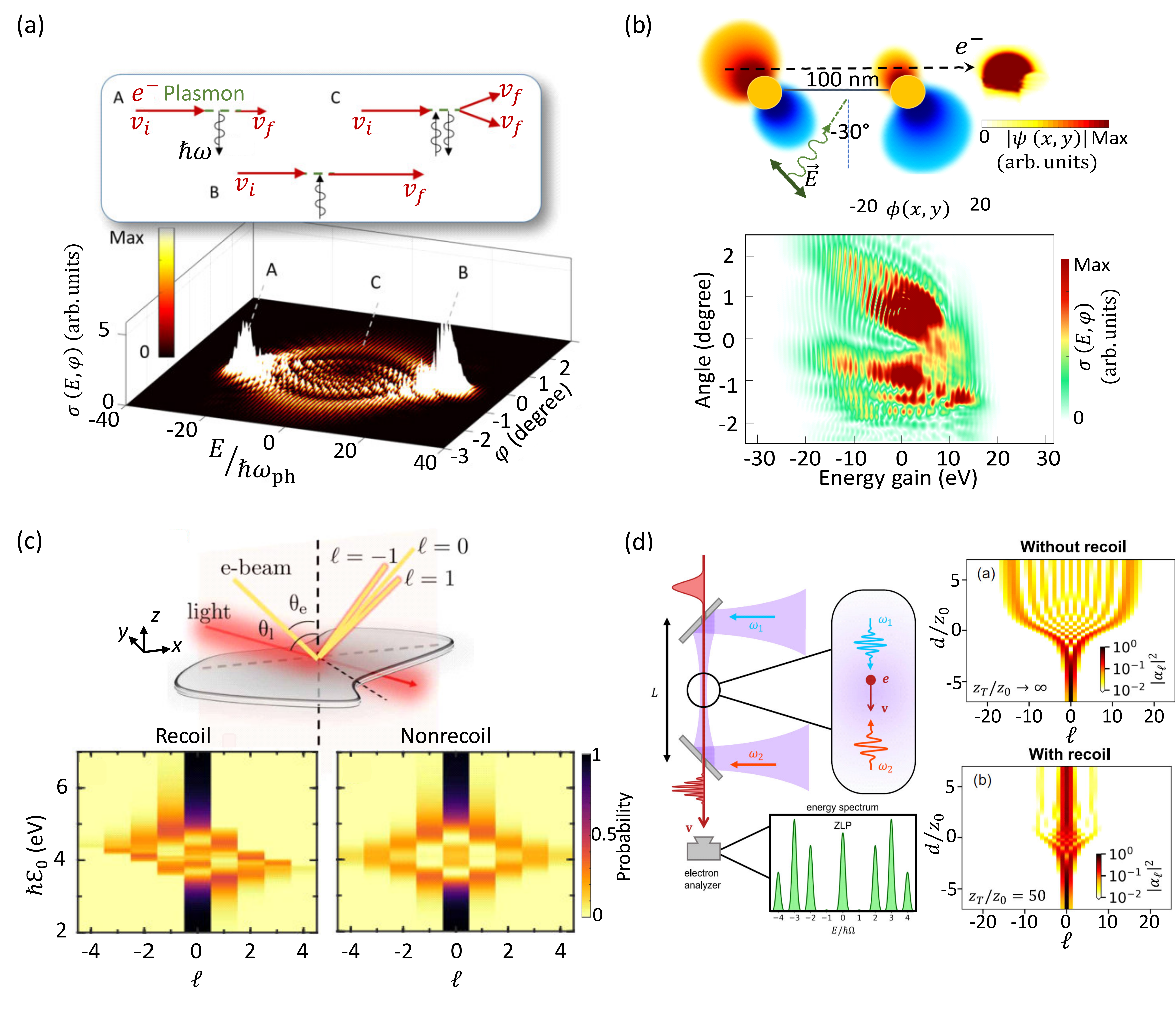
Optimizing electron beam characteristics in Photon-Induced Near-Field Electron Microscopy (PINEM) relies heavily on techniques such as wavepacket and electron beam shaping, both fundamentally driven by the \nabla E \times B ponderomotive force. Wavepacket shaping manipulates the temporal and spatial characteristics of the electron wavepacket to enhance interaction with the near-field optical excitation, increasing signal amplitude and coherence. Simultaneously, electron beam shaping focuses on minimizing aberrations and maximizing current density at the sample, achieved through electrostatic and magnetic lens control. Precise manipulation of the electron beam, guided by the ponderomotive force, allows for targeted excitation of near-field enhanced regions, improving spatial resolution and signal-to-noise ratio, and is critical for maximizing the efficiency of photoemission processes in PINEM.
The recoil effect in Photon-Induced Near-Field Electron Microscopy (PINEM) arises from the momentum transfer during photon-electron interactions, complicating image interpretation and signal optimization. When a photon interacts with an electron, the electron gains momentum from the photon, resulting in a recoil event that can displace the electron from the desired imaging plane or alter its trajectory. The magnitude of this recoil is directly proportional to the photon energy and inversely proportional to the electron momentum; therefore, minimizing photon energy and maximizing electron momentum are crucial for mitigating the recoil effect. Careful consideration of these parameters is required to ensure accurate data acquisition and to prevent signal degradation, particularly when aiming for high-resolution imaging of delicate samples or buried interfaces.
Attosecond temporal resolution in photon-induced near-field electron microscopy (PINEM) is achieved by precisely controlling and compressing electron wavepackets using light. This is accomplished through techniques such as femtosecond laser-induced photoemission and subsequent acceleration of electrons within nanostructured near-field environments. The process leverages the interaction between photons and electrons to manipulate the electron’s momentum distribution, effectively shortening the duration of the electron wavepacket. Specifically, the use of high harmonic generation to produce attosecond pulses, combined with optimized electron optics and time-of-flight spectroscopy, enables the observation of ultrafast dynamics at the atomic scale. Current systems have demonstrated resolutions on the order of 10^{-{16}} seconds, facilitating the study of electron correlation and transient phenomena in materials.
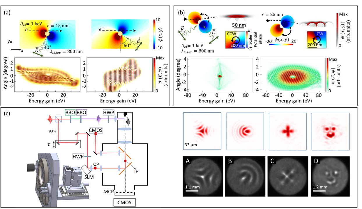
Nanometer-scale spatial resolution in Photon-Induced Near-Field Electron Microscopy (PINEM) is achieved through the synergistic effect of near-field coupling and specifically designed nanophotonic structures. Near-field coupling concentrates the electromagnetic field beyond the diffraction limit, enhancing the interaction between photons and electrons at the sample surface. This is further optimized by employing nanophotonic structures – such as plasmonic antennas or dielectric resonators – which facilitate localized field enhancements and direct energy transfer to the electron beam. These structures enable precise control over the spatial distribution of the electromagnetic field, allowing for imaging with resolutions approaching a few nanometers and facilitating the investigation of materials at the nanoscale.

Beyond Resolution: Implications and Future Directions
The relentless pursuit of higher resolution and increased sensitivity in electron microscopy is now revealing the inner workings of materials at previously inaccessible timescales. Researchers are moving beyond static snapshots to observe dynamic processes – such as phase transitions, chemical reactions, and the behavior of defects – as they unfold in real-time. This capability isn’t merely about seeing smaller features; it’s about understanding how materials change and respond to external stimuli. By capturing these fleeting events with atomic precision, scientists can validate theoretical models, discover new phenomena, and ultimately engineer materials with tailored properties. The ability to directly visualize these dynamic processes promises breakthroughs in fields ranging from catalysis and energy storage to materials science and nanotechnology, offering insights that were once confined to computational simulations.
Electron microscopy stands to gain significantly from advancements in controlling the quantum coherence of electron beams. Typically treated as classical particles, electrons exhibit wave-like properties, including coherence, which dictates the phase relationship between different parts of the electron wave. Maintaining and manipulating this coherence allows for the creation of electron beams with tailored properties, dramatically enhancing image contrast and resolution-potentially circumventing the limitations imposed by chromatic and spherical aberrations. Furthermore, coherent electron beams open doors to novel spectroscopic techniques, such as electron diffraction with vastly improved signal-to-noise ratios and the potential to probe materials’ electronic structure with unprecedented precision. This control isn’t merely about achieving sharper images; it allows researchers to leverage the full quantum mechanical nature of the electron, unlocking capabilities for studying delicate quantum phenomena within materials and pushing the boundaries of materials science and nanotechnology.
Accurate interpretation of electron microscopy images hinges on a thorough understanding of scattering asymmetry – the preferential deflection of electrons in certain directions by a material. This phenomenon arises because heavier atoms scatter electrons more strongly than lighter ones, and the scattering angle depends on the atomic number. Failing to account for this asymmetry leads to distortions in the reconstructed image, obscuring fine details and potentially misrepresenting material composition. Researchers are actively developing advanced algorithms and beam shaping techniques to correct for these asymmetries, effectively ‘equalizing’ the scattering contribution from different elements. By precisely controlling the electron beam and modeling the scattering process, it becomes possible to enhance image contrast, improve resolution, and ultimately gain more reliable insights into the structure and properties of the sample under investigation. Improved modeling of \text{scattering asymmetry} is therefore central to pushing the boundaries of what can be observed with electron microscopy.
A cornerstone of efficient electron microscopy data analysis lies in the widespread applicability of the non-relativistic electron approximation. This simplification, which treats electrons as moving at speeds significantly below that of light, dramatically reduces the computational complexity of modeling electron beam interactions with matter. While relativistic effects become important at very high accelerating voltages, for a vast range of practical applications – including many materials science and biological investigations – the approximation provides remarkably accurate results. This allows researchers to focus computational resources on refining other aspects of image reconstruction and analysis, such as aberration correction and signal processing, rather than on solving complex relativistic equations. Consequently, the non-relativistic treatment facilitates rapid data processing and interpretation, accelerating scientific discovery in fields reliant on high-resolution electron imaging and spectroscopy.
Recent advancements demonstrate the feasibility of programmable wavepacket shaping control, a technique poised to revolutionize electron microscopy. This capability allows for the precise tailoring of electron beams – not simply in intensity, but in their complete wave-like profile – enabling researchers to sculpt beams optimized for specific materials and imaging conditions. By dynamically manipulating the phase and amplitude of the electron wave, aberrations – distortions that blur images – can be actively corrected in real-time. Furthermore, custom beam profiles can be created to enhance contrast, improve signal-to-noise ratios, and even probe specific atomic or electronic states within a sample. This level of control moves beyond simply focusing the beam; it allows for the creation of bespoke illumination tools, promising substantial gains in resolution, sensitivity, and the ability to perform novel spectroscopic analyses at the nanoscale.
![Applying a Laguerre-Gaussian laser beam creates an optical field electron mirror (OFEM) that corrects spherical aberration and restores undistorted fringes, as demonstrated by the correction of an aberrated beam <span class="katex-eq" data-katex-display="false"> ightarrow</span> corrected image (reproduced with permission from Nature Photonics [21] under CC BY 4.0).](https://arxiv.org/html/2602.17463v1/finall2.png)
The pursuit of controlling electron behavior with light, as detailed in the review of stimulated electron-light interactions, mirrors a dedication to fundamental correctness. Grigori Perelman once stated, “If you don’t understand something, you need to go back and learn it again.” This sentiment resonates deeply with the meticulous work described, where achieving precise phase control and mitigating recoil effects aren’t merely practical goals, but demands for provable, reproducible results. The ability to shape electron beams and induce stimulated emission isn’t about creating a ‘working’ system; it’s about establishing a demonstrably correct one, governed by the unwavering laws of physics. Any deviation from this principle undermines the reliability of the advancements in imaging and quantum technologies.
Where Does This Leave Us?
The pursuit of coherent control over electrons via light, as detailed in this review, has yielded intriguing results. Yet, it is crucial to acknowledge that ‘control’ remains a loosely defined term. Demonstrating correlation between stimulated emission and beam shaping is not, in itself, proof of deterministic manipulation. The field currently relies heavily on empirical observation; a rigorous mathematical framework capable of predicting electron behavior under arbitrary light fields is notably absent. Until such a formalism emerges, the assertion of genuine control remains, at best, a compelling conjecture.
A significant limitation lies in the treatment of recoil effects. Current models often simplify these interactions, treating the electron as a point particle. A more complete description necessitates incorporating relativistic corrections and accounting for the internal structure of the electron itself – a pursuit bordering on the metaphysical, perhaps, but essential for true predictive power. Furthermore, the scaling of these techniques to more complex systems – from single electrons to coherent beams comprising vast numbers of particles – presents formidable challenges.
The future likely resides in bridging the gap between theoretical elegance and experimental feasibility. While the prospect of ‘quantum imaging’ and ‘stimulated spectroscopy’ is alluring, these remain aspirations contingent upon establishing a truly provable – not merely demonstrable – understanding of electron-light interactions. The field must prioritize the derivation of first-principles equations over the accumulation of empirical data; otherwise, it risks becoming a collection of fascinating observations lacking fundamental grounding.
Original article: https://arxiv.org/pdf/2602.17463.pdf
Contact the author: https://www.linkedin.com/in/avetisyan/
See also:
- What Song Is In The New Supergirl Trailer (& What It Means For The DC Movie)
- Eurogamer Gives ARC Raiders 2/5 Over AI Voices, Dropping Metacritic Score from 94 to 84
- Gold Rate Forecast
- FRONT MISSION 3: Remake coming to PS5, Xbox Series, PS4, Xbox One, and PC on January 30, 2026
- Miss Super Sentai After Cancellation? Watch These 5 Anime to Fill the Void
- Teresa Giudice’s Real Housewives Season One Salary Revealed
- Starfield PS5 Won’t Play Off Physical Disc without a Download
- After 13 Years, Someone Earned One of the Hardest Achievement Trophies in Gaming
- Global Easing Boils Over – So Why Is Bitcoin Still Playing Hard to Get?
- The Simpsons Makes Major Change to Patty and Selma After 36 Years (And Includes a Big Makeover)
2026-02-20 14:53