Author: Denis Avetisyan
A new silicon-based photonic crystal cavity enables highly sensitive, frequency-domain detection of nanoscale material properties at cryogenic temperatures.
Researchers demonstrate sensitive perturbation sensing of multilayer graphene flakes using millimeter-wave photonics and silicon-on-insulator technology.
Characterizing nanoscale materials in extreme environments requires sensing techniques compatible with high magnetic fields-a limitation for conventional superconducting resonators. Here, we present ‘Perturbative sensing of nanoscale materials with millimeter-wave photonic crystals’, demonstrating a silicon-on-insulator platform utilizing millimeter-wave photonic crystal cavities for sensitive, frequency-domain material characterization. We achieve quality factors exceeding 10^5 at cryogenic temperatures and successfully measure the conductivity of a hexagonal boron nitride-multilayer graphene heterostructure. Could this dielectric approach unlock new avenues for studying quantum materials and exploring emergent phenomena at the nanoscale?
Decoding the Limits of Perception: Nanoscale Sensing with Photonic Structures
The pursuit of increasingly precise material characterization necessitates sensors capable of resolving changes at the nanoscale, demanding both exceptional resolution and sensitivity. Detecting alterations in material properties – such as strain, composition, or the presence of a single dopant atom – requires a device that can discern exceedingly faint signals. Conventional sensing techniques often struggle with this task, limited by diffraction or a lack of inherent sensitivity to subtle shifts. Therefore, advancements in nanotechnology are focused on creating sensors that can not only pinpoint the location of a change with nanometer precision but also accurately quantify its magnitude, opening doors to a deeper understanding of material behavior and enabling the development of novel devices with tailored functionalities.
The characterization of two-dimensional materials, such as graphene, presents a significant challenge to conventional sensing techniques. Traditional methods, often relying on macroscopic measurements or techniques with limited spatial resolution, struggle to detect the subtle changes in physical or chemical properties that define these atomically thin layers. Graphene, for example, exhibits extraordinary sensitivity to even single dopant atoms or adsorbed molecules, effects that are easily masked or lost when probed with instruments designed for bulk materials. This limitation hinders fundamental research into their unique properties and impedes the development of advanced devices dependent on precise material control. Consequently, there is a growing need for sensing platforms capable of resolving nanoscale variations in these materials with unprecedented precision and sensitivity.
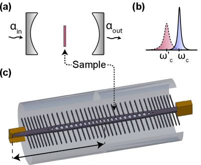
Silicon photonic crystal cavities present a novel approach to perturbative sensing, achieving resolutions on the order of 100 GHz by meticulously controlling light at the nanoscale. These structures, engineered with periodic variations in refractive index, act as optical resonators, trapping light within a tiny volume. When a material is introduced near this confined light, it subtly alters the cavity’s resonant frequency – a measurable shift proportional to the material’s properties or changes within it. This sensitivity arises from the strong light-matter interaction facilitated by the cavity’s ability to concentrate electromagnetic fields. By precisely monitoring these frequency shifts, researchers can detect even minute alterations in the target material, opening possibilities for high-resolution material characterization and sensing applications beyond the reach of traditional methods.
Silicon photonic crystal cavities operate as remarkably sensitive perturbative sensors by meticulously tracking alterations in their resonant frequencies. These cavities, engineered to confine light within extremely small volumes, exhibit a strong response to even minute changes in their surrounding environment. When a material approaches the cavity, it subtly perturbs the electromagnetic field, causing a measurable shift in the wavelengths of light that resonate within the structure. This frequency shift is directly proportional to the material’s properties – its refractive index, thickness, or even its chemical composition – allowing for non-destructive, nanoscale characterization. The precision of this method stems from the cavity’s ability to amplify the interaction between light and the target material, effectively turning the cavity into a highly sensitive detector of external influences.
Sculpting with Shadows: Nanofabrication via Reactive-Ion Etching
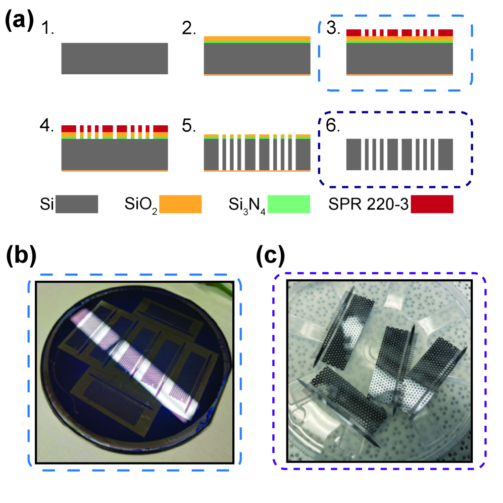
Silicon photonic crystal cavity fabrication utilizes dry etching techniques, with reactive-ion etching (RIE) being the predominant method. RIE involves subjecting a silicon wafer to a plasma containing chemically reactive ions; these ions selectively remove silicon material based on the masking layer applied to the surface. Unlike wet etching, dry etching offers anisotropic etching profiles, enabling precise control over feature shapes and sizes at the nanoscale. The process typically employs gases such as sulfur hexafluoride (SF_6) or chlorine (Cl_2) combined with argon (Ar) to generate the etching plasma, and is conducted under vacuum to ensure directional etching and minimize undercutting, critical for defining the periodic structures necessary for photonic crystal functionality.
Deep reactive-ion etching (DRIE) is a specialized dry etching process that significantly expands the fabrication possibilities for silicon photonic crystals. Unlike conventional reactive-ion etching, DRIE utilizes a cyclical process of etching and passivation – typically the Bosch process – to achieve nearly vertical sidewalls and enable the creation of structures with high aspect ratios, defined as the ratio of structure height to width. These high-aspect-ratio features are critical for maximizing light confinement within the photonic crystal cavities; a greater height-to-width ratio increases the effective refractive index contrast, leading to stronger localization of light and improved cavity performance. The ability to reliably fabricate these deep, narrow features is essential for realizing efficient and compact silicon photonic devices.
The fabrication of photonic crystal cavities utilizes reactive-ion etching to precisely remove silicon material, creating a periodic arrangement of holes within a silicon substrate. This periodic structure is fundamental to the formation of a photonic bandgap – a range of frequencies where electromagnetic waves are prevented from propagating. The dimensions and spacing of these etched holes directly influence the size and position of the bandgap, and therefore the optical properties of the resulting cavity. By carefully controlling the etching process, the periodic arrangement is defined with nanometer-scale precision, enabling the creation of cavities capable of strongly confining light at specific wavelengths.
Achieving optimal photonic crystal cavity characteristics during nanofabrication necessitates precise control of reactive-ion etch (RIE) parameters. Specifically, gas composition-typically a mixture of SF_6 and O_2-influences etch rate and selectivity; higher SF_6 flow rates generally increase the etch rate of silicon, while O_2 passivates the silicon surface, reducing etch rate and enabling anisotropic etching. Radio-frequency (RF) power dictates the plasma density and ion energy, impacting both etch rate and sidewall profile. Pressure affects the mean free path of ions, influencing directionality and uniformity. Finally, temperature control is critical as it influences chemical reaction rates and can affect etch selectivity and feature profiles; deviations from optimal temperatures can lead to undercutting, bowing, or non-uniformity, ultimately degrading cavity performance.
The Resonance of Perfection: Maximizing Quality Factor for Sensitivity
The quality factor, Q, of a photonic crystal cavity is a dimensionless parameter that quantifies the ratio of stored energy to energy lost per optical cycle. A higher Q indicates lower energy dissipation and, consequently, a sharper resonance. This is directly relevant to sensitivity because a narrow resonance is more susceptible to shifts caused by changes in the surrounding environment; even minute perturbations – such as the binding of a target molecule or a slight refractive index change – will result in a measurable spectral shift. Therefore, maximizing Q is crucial for applications involving sensing and precise spectroscopic measurements, as it enhances the cavity’s ability to detect weak external influences.
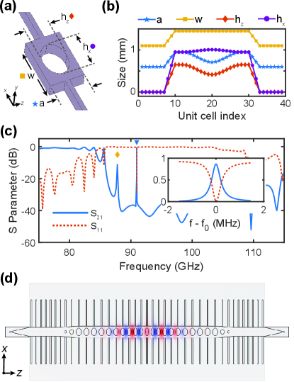
The optimization of the photonic crystal cavity’s radiation-limited quality factor (Q) was achieved through the implementation of a genetic algorithm. This computational method iteratively refined the geometric parameters of the cavity design, specifically focusing on the defect mode responsible for light confinement. The algorithm operated by evaluating the Q factor for a population of cavity designs, selecting those with higher values, and then introducing variations – mutations and crossovers – to generate subsequent generations. This process continued until a design maximizing the radiation-limited Q was obtained, minimizing light leakage and enhancing cavity performance. The resulting geometry was then fabricated and experimentally verified.
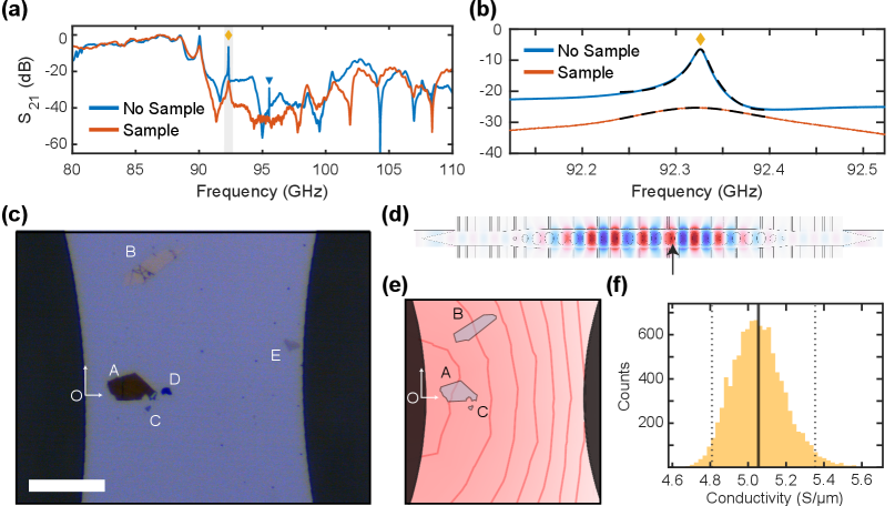
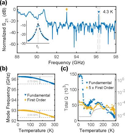
Characterization of the fabricated photonic crystal cavity was conducted at cryogenic temperatures using a WR10 waveguide to accurately assess its performance in a low-temperature environment. The WR10 waveguide, operating within the 75-110 GHz (W-band) frequency range, facilitated efficient coupling to the cavity mode for precise spectral analysis. Measurements were taken at 4.3 K to minimize thermal noise and maximize the signal-to-noise ratio, allowing for a detailed evaluation of the cavity’s resonant frequency and quality factor. This setup enabled the determination of the bare cavity’s intrinsic properties, excluding any external perturbations, and established a baseline for subsequent sensing experiments conducted at similar temperatures.
Characterization of the fabricated photonic crystal cavity via cryogenic measurements using a WR10 waveguide confirmed a high internal quality factor (Q) of 1.7 x 10⁵ at a temperature of 4.3 K. This high-Q resonance was achieved within the W-band frequency range of 75-110 GHz, demonstrating the cavity’s ability to support high-finesse resonances at these frequencies. The resulting performance metrics establish a crucial baseline for evaluating the sensitivity and performance of subsequent sensing experiments utilizing this cavity design.
Unveiling the Invisible: Material Characterization with Multilayer Graphene
Multilayer graphene emerged as a compelling material for sensing applications due to its exceptional electronic characteristics. Unlike single-layer graphene, multilayer graphene exhibits tunable electronic properties dependent on the number of layers and stacking order, allowing for enhanced sensitivity and selectivity in sensing mechanisms. This material presents a high carrier mobility and a density of states that can be engineered to respond to a wide range of stimuli, including changes in chemical environment or mechanical stress. The inherent two-dimensional nature of graphene, even in its multilayer form, facilitates strong light-matter interactions, crucial for photonic sensing platforms, and allows for efficient charge transport, which is essential for electrical detection schemes. Consequently, multilayer graphene provides a versatile platform for developing highly sensitive and responsive sensors across various disciplines, from environmental monitoring to biomedical diagnostics.
The successful integration of multilayer graphene with the silicon photonic crystal cavity necessitated a precise transfer technique, achieved through the utilization of hexagonal boron nitride (hBN) as a pick-up layer. This approach leveraged hBN’s atomically flat surface and weak van der Waals interactions with both the graphene and the silicon substrate, enabling gentle release and subsequent placement of the graphene flake. Essentially, the hBN acted as a temporary support, preventing damage during the detachment from its growth substrate and allowing for controlled deposition onto the target cavity structure with minimal contamination – a crucial step for maintaining the integrity of the photonic crystal and ensuring reliable sensing measurements.
To characterize the electrical properties of multilayer graphene, researchers employed cavity perturbation theory, a technique leveraging the sensitivity of a photonic crystal cavity to nearby materials. This approach, grounded in the Drude model-which describes the frequency-dependent conductivity of materials-allowed for the extraction of the graphene’s complex permittivity and permeability. By analyzing the shifts and broadening of the cavity’s resonant modes caused by the graphene’s presence, the material’s dielectric and magnetic responses could be determined without direct contact. This method effectively transforms the graphene flake into a miniature dielectric object whose properties subtly alter the cavity’s electromagnetic environment, providing a sensitive means of characterizing its fundamental electrical behavior.
Detailed characterization of the multilayer graphene flakes was achieved through microwave impedance microscopy, confirming both their physical attributes and key electrical properties. Measurements established a conductivity of 5.1 \times 10^6 S/m, demonstrating the material’s potential for high-performance applications, with a statistically significant 95% confidence interval ranging from 4.8 \times 10^6 to 5.4 \times 10^6 S/m. The presence of these graphene flakes notably perturbed the silicon photonic crystal cavity, inducing a measurable frequency shift of 2\pi \times 2 MHz and broadening the cavity linewidth by 2\pi \times 129 MHz; these shifts provide valuable insight into the graphene’s dielectric environment and its interaction with the cavity structure.
The research meticulously details a system designed for precise material characterization, probing graphene’s properties at millimeter wavelengths. This pursuit of quantifiable data, achieved through a silicon-based photonic crystal cavity, inherently involves a process of controlled disruption. As Blaise Pascal observed, “The eloquence of angels is silence.” This seemingly paradoxical statement resonates with the methodology; it is in the subtle perturbations-the minute shifts in frequency and response-that the system reveals its secrets. The cavity doesn’t simply observe graphene; it actively elicits a response, a confession of the material’s intrinsic characteristics, akin to a bug revealing the system’s design flaws. The high quality factors achieved at cryogenic temperatures simply amplify this subtle dialogue.
Beyond the Resonance
The demonstration of millimeter-wave photonic crystal cavities as perturbation sensors reveals a curious truth: sensitivity often arises not from perfect isolation, but from exquisitely controlled interaction. One begins to wonder if the ‘noise’ inherent in material characterization – the subtle variations dismissed as imperfections – might, in fact, be the most informative signals. The current iteration, focused on graphene, is merely a proof of concept. The real challenge lies in expanding this approach to materials where the expected response is… less cooperative. What happens when the perturbation isn’t a simple shift in resonant frequency, but a complete reshaping of the electromagnetic landscape?
The cryogenic environment, while enhancing quality factors, introduces its own constraints. Future iterations should explore operation at higher temperatures, trading some sensitivity for practicality. More provocatively, one could consider intentionally introducing disorder into the photonic crystal itself. A perfectly periodic structure is, after all, an idealized abstraction. Perhaps a carefully engineered degree of imperfection would unlock new sensing modalities, allowing the cavity to ‘learn’ the properties of the material under investigation.
This work isn’t about building better sensors, necessarily. It’s about questioning what ‘characterization’ truly means. If a material doesn’t respond as expected, does that indicate a flaw in the material, or a limitation in the measurement technique? The most fruitful path forward may lie in embracing the unexpected, treating anomalies not as errors to be corrected, but as invitations to a deeper understanding.
Original article: https://arxiv.org/pdf/2602.17527.pdf
Contact the author: https://www.linkedin.com/in/avetisyan/
See also:
- What Song Is In The New Supergirl Trailer (& What It Means For The DC Movie)
- TV legend Carol Kirkwood reveals the reasons why she decided to retire after 28 years with BBC
- Dune 3 Gets the Huge Update Fans Have Been Waiting For
- Highly Anticipated Strategy RPG Finally Sets Release Date (And It’s Soon)
- The Super Mario Galaxy Movie: 50 Easter Eggs, References & Major Cameos Explained
- Why is Tech Jacket gender-swapped in Invincible season 4 and who voices her?
- Welcome to Demon School! Iruma-kun season 4 release schedule: When are new episodes on Crunchyroll?
- Sydney Sweeney’s The Housemaid 2 Sets Streaming Release Date
- Who Wants to Be a Millionaire? confirms contestant wins full £1 million prize pot on Jeremy Clarkson quiz
- The OG Resident Evil 1, 2 and 3 Are Now Available on Steam With a Heavy Discount (and DRM)
2026-02-21 14:23