Author: Denis Avetisyan
New research directly observes impurity states within an excitonically insulating material, confirming the role of charge dipoles formed by material vacancies.
Observation of Yu-Shiba-Rusinov bound states in Ta2Pd3Te5 provides strong evidence for an exciton-driven insulating phase.
The elusive connection between impurity states and quantum condensation remains a central challenge in condensed matter physics. Here, we report on the observation and characterization of Yu-Shiba-Rusinov bound states within the exciton condensate phase of the van der Waals material Ta₂Pd₃Te₅, as detailed in ‘Yu-Shiba-Rusinov bound states of exciton condensate’. Utilizing scanning tunneling microscopy and spectroscopy, we demonstrate that these in-gap states arise from charge dipoles associated with native Ta vacancies, confirming the excitonic origin of the insulating phase. Could manipulating these defect-induced states offer a pathway to control and probe the unique quantum properties of exciton condensates, even at room temperature?
The Excitonic Insulator: A Departure from Conventionality
Ta2Pd3Te5, a layered van der Waals material, challenges conventional understandings of insulation through its realization of an excitonic insulator phase. Unlike typical insulators which derive their properties from a large energy gap separating filled and empty electron bands, this material’s insulating behavior arises from strong electron interactions. These interactions don’t block electron movement directly, but instead promote the formation of tightly bound electron-hole pairs called excitons. At low temperatures, these excitons undergo a phase transition, condensing into a collective quantum state that effectively prevents electrical conduction – a phenomenon distinct from band-gap-driven insulation. This unique mechanism, where correlated electron behavior creates the insulating state, positions Ta2Pd3Te5 as a promising platform for exploring novel quantum phases and devices, differing significantly from traditional semiconductor materials.
Ta2Pd3Te5 distinguishes itself from typical insulators through a fascinating state driven by collective exciton condensation. In conventional insulators, electrons are individually blocked from conducting electricity; however, within this excitonic insulator, electrons pair up to form excitons – bound electron-hole pairs – which then condense into a coherent quantum state. This isn’t simply a reduction in conductivity, but a fundamentally different organization of electronic behavior, where interactions between electrons dictate the material’s properties. The resulting macroscopic quantum state opens pathways to observe and potentially harness novel phenomena, including topologically protected edge states and unconventional superconductivity, making this material a promising arena for exploring advanced quantum technologies and pushing the boundaries of condensed matter physics.
The promise of Ta2Pd3Te5 as a platform for quantum technologies hinges on the delicate excitonic insulator phase it exhibits, but this phase is acutely sensitive to imperfections within the material’s structure. Defects, even at low concentrations, can disrupt the collective exciton condensation responsible for the insulating behavior, potentially collapsing this quantum state. Consequently, a thorough understanding of how these defects-ranging from missing atoms to structural distortions-modify the electronic landscape is paramount. Researchers are actively investigating defect engineering strategies, aiming to either minimize their detrimental effects or, conversely, harness them to tailor the material’s properties for specific quantum applications, such as developing novel spintronic devices or realizing topologically protected quantum states.
The delicate excitonic insulating phase in Ta2Pd3Te5 is acutely sensitive to imperfections within its atomic structure. Even a small concentration of defects-vacancies, interstitials, or substitutional impurities-can profoundly reshape the material’s electronic landscape. These deviations from perfect crystallinity disrupt the subtle balance driving exciton condensation, potentially collapsing the insulating state or introducing localized states that alter charge transport. Consequently, a thorough investigation of defect characteristics-their type, concentration, and spatial distribution-is paramount. Advanced characterization techniques, coupled with theoretical modeling, are essential to unravel how these imperfections influence the electronic band structure, exciton properties, and ultimately, the potential of this material for realizing novel quantum devices. Understanding and controlling these defects represents a critical step towards harnessing the unique properties of this excitonic insulator.

Unveiling the Role of Tantalum Vacancies
Tantalum vacancies within the Ta_2Pd_3Te_5 crystal structure introduce localized disruptions to the material’s electronic structure through the formation of charge dipoles. These vacancies, representing missing tantalum atoms in the lattice, create an uneven distribution of electron density. First-principles calculations demonstrate that the introduction of a single tantalum vacancy results in a charge displacement, generating a dipole moment. This deviation from the ideal, stoichiometric arrangement directly impacts the surrounding electronic environment, altering the band structure and influencing the material’s overall electronic properties. The presence of these induced dipoles represents a significant departure from the pristine, undisturbed electronic configuration of the Ta_2Pd_3Te_5 compound.
First-principles Density Functional Theory (DFT) calculations were employed to model the atomic structure and electronic properties of tantalum (Ta) vacancies within the Ta_2Pd_3Te_5 compound. This computational approach solves the Schrödinger equation based on fundamental physical constants, without empirical parameters, to determine the ground state electronic structure. The methodology utilizes a plane-wave basis set and the generalized gradient approximation (GGA) for the exchange-correlation functional. Validation of the DFT setup involved convergence testing of k-point sampling and energy cutoff parameters to ensure numerical accuracy. The resulting models accurately reproduce the crystallographic structure and provide a reliable framework for investigating the electronic effects of Ta vacancies, including charge redistribution and the formation of in-gap states.
Density Functional Theory (DFT) calculations demonstrate that tantalum (Ta) vacancies in Ta2Pd3Te5 generate a charge dipole with a magnitude of -0.45 x 10⁻¹² C⋅m. This dipole moment arises from the redistribution of electron density following Ta atom removal, creating a localized separation of positive and negative charge. The resulting electric field significantly modifies the electronic structure in the immediate vicinity of the vacancy, perturbing the potential experienced by neighboring electrons and influencing the material’s electronic properties. This alteration extends beyond a simple potential shift, leading to measurable changes in the local density of states and contributing to the formation of in-gap states.
The formation of tantalum vacancy-induced charge dipoles within Ta2Pd3Te5 leads to the creation of localized electronic states appearing within the material’s excitonic gap. These in-gap states, resulting from the disruption of the electronic band structure, are confined to the immediate vicinity of the tantalum vacancy. Calculations indicate these states reside approximately 100 meV within the band gap, effectively reducing the energy required for electronic transitions in that localized region and altering the material’s optical and electrical properties. The presence of these states contributes to increased conductivity and modifies the material’s response to external stimuli.

Direct Observation: Mapping Localized States
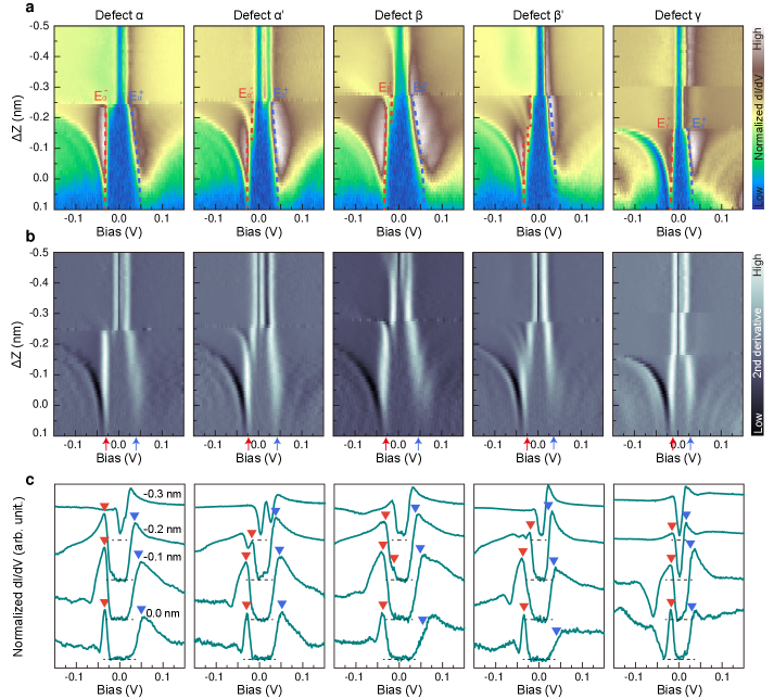
Scanning Tunneling Microscopy (STM) operates by measuring the tunneling current between a sharp metallic tip and the sample surface, a current directly proportional to the local density of electronic states (LDOS) at the tip’s location. In the context of tantalum vacancies, STM images reveal spatial variations in LDOS arising from the disruption of the material’s electronic band structure. Specifically, the induced in-gap states – energy levels appearing within the band gap – manifest as distinct features in the STM images due to their altered LDOS. By rastering the tip across the surface, STM effectively maps the spatial distribution of these in-gap states, allowing for direct visualization of their localization around the Ta vacancy sites. The tunneling current is highly sensitive to changes in LDOS even at the atomic scale, providing a robust method for probing these localized electronic features.
Scanning Tunneling Microscopy (STM) measurements directly reveal the presence of localized electronic states appearing within the material’s excitonic gap. These states are not delocalized across the material, but instead exhibit a strong spatial correlation with the location of tantalum (Ta) vacancies. Specifically, STM data demonstrates that an increase in local density of states occurs at the site of each Ta vacancy, indicating the formation of in-gap states due to the disrupted crystal lattice. The measured spatial distribution of these states confirms their confinement to the immediate vicinity of the defects, with the signal diminishing rapidly with distance from the vacancy site. This observation supports the theoretical prediction of defect-induced localized states within the band gap.
Angle-Resolved Photoemission Spectroscopy (ARPES) provides a comprehensive mapping of the material’s electronic band structure, which complements the localized information obtained from Scanning Tunneling Microscopy (STM). ARPES measurements determine the energy and momentum of emitted electrons, revealing the dispersion relations of the electronic bands. Analysis of these spectra confirms the disruption of the band structure induced by Ta vacancies, evidenced by the appearance of defect-related bands or modifications to existing band dispersions. Specifically, ARPES data validates the impact of these defects on the overall electronic structure, corroborating the presence of in-gap states and providing a broader context for the localized states observed via STM. This combined approach allows for a complete understanding of both the local and global electronic effects of Ta vacancies.
Analysis of Scanning Tunneling Microscopy (STM) topography revealed local strain variations of 2.4% surrounding tantalum (Ta) vacancies. This quantification was achieved through the application of a two-dimensional Fast Fourier Transform (2D FFT) filtering technique to the STM data. The 2D FFT allows for the mapping of periodic distortions in the surface lattice, and its application specifically identified strain fields induced by the presence of the Ta vacancies. This measurement provides insight into the defect environment, indicating a localized distortion of the material’s crystal lattice around each vacancy and contributing to a more complete understanding of the in-gap state formation.
The convergence of Scanning Tunneling Microscopy (STM), Angle-Resolved Photoemission Spectroscopy (ARPES), and two-dimensional Fast Fourier Transform (2D FFT) analysis of STM topography provides corroborating evidence for the formation of in-gap states induced by charge dipoles. STM directly visualizes these states as localized variations in the local density of states. ARPES confirms the broader impact of these defects on the material’s band structure, while 2D FFT filtering of STM data quantifies local strain variations – measured at 2.4% – surrounding the vacancies. This combined approach establishes a strong correlation between the presence of Ta vacancies, induced strain, and the resulting spatially localized electronic states within the excitonic gap.

Towards Novel Quantum Phases: Implications and Analogies
The emergence of in-gap states induced by charge dipoles within the exciton condensate shares a striking resemblance to the well-known Yu-Shiba-Rusinov (YSR) resonances observed in conventional superconductors containing magnetic impurities. YSR resonances arise from the scattering of Cooper pairs by localized magnetic moments, creating bound states within the superconducting gap. Similarly, the charge impurity in this system functions as a scattering center for the exciton condensate, disrupting the condensate’s coherence and inducing localized states at energies within the exciton gap. This analogous behavior suggests a shared underlying physics-the formation of bound states due to the scattering of bosonic condensates by localized defects-and opens the possibility of leveraging insights from superconductivity to understand and manipulate these exciton-based states. The spectral features of these in-gap states, specifically their energy dependence and spatial localization, closely mirror those predicted and experimentally observed for YSR resonances, further solidifying this compelling connection.
The behavior of charge impurities within the exciton condensate strikingly parallels the role of magnetic impurities in conventional superconductivity. Just as magnetic impurities disrupt Cooper pair formation, leading to localized states and scattering, these charged defects act as scattering centers for the exciton condensate. This disruption isn’t a simple energy loss; rather, it induces localized, in-gap states – energy levels appearing within the band gap of the material. The impurity’s charge alters the local potential, effectively ‘trapping’ excitons and creating these states, mirroring the Yu-Shiba-Rusinov (YSR) resonances seen when magnetic impurities break Cooper pairs and induce bound states near the Fermi level in superconductors. Understanding this analogy is crucial, as it suggests that controlling charge impurities offers a pathway to manipulate and engineer the properties of the exciton condensate, potentially leading to novel quantum phenomena.
The emergence of in-gap states within the quantum contact regime signifies a substantial interplay between the introduced charge impurity and the surrounding exciton condensate. This isn’t merely a perturbative effect; rather, the observation indicates that the impurity fundamentally alters the condensate’s properties, creating localized states where excitons are effectively trapped or scattered. The strength of this interaction is evidenced by the distinct spectral features of these in-gap states, which deviate significantly from predictions based on weak coupling models. This strong coupling regime suggests a hybridization between the impurity’s electronic states and the exciton condensate, leading to a collective behavior where the impurity and condensate act as a single, coupled quantum system. Consequently, the charge impurity effectively functions as a localized potential well, modulating the exciton density and potentially inducing novel quantum phases beyond the standard exciton condensate.
The absence of Zeeman splitting in the observed in-gap states, even when subjected to magnetic fields as high as 2.5 Tesla, points to a distinctly non-conventional character for these quantum phenomena. Typically, Zeeman splitting – the separation of energy levels in a magnetic field – is a hallmark of states with spin angular momentum. The lack of this splitting suggests the in-gap states are either devoid of net spin, or that the spin is effectively decoupled from the external magnetic field due to unique interactions within the system. This decoupling challenges conventional understandings of spin behavior in condensed matter and implies a novel mechanism governing the formation and properties of these in-gap states, potentially linked to their topological origin and hinting at the possibility of robust, spin-insensitive quantum information processing.
The emergence of in-gap states induced by charge dipoles suggests a pathway towards realizing topological exciton insulator phases – a novel state of matter with potentially groundbreaking properties. Unlike conventional insulators, these phases are predicted to host robust, conducting edge states, protected from backscattering and imperfections, allowing for dissipationless current flow. These edge states arise from the unique topological properties of the exciton condensate, where the interplay between charge impurities and excitons creates a non-trivial band structure. Such phases promise a range of quantum phenomena, including fractionalized excitations and enhanced sensitivity to external stimuli, potentially enabling advancements in quantum computing, spintronics, and low-power electronics. Further investigation into controlling and manipulating these topological exciton insulator phases could unlock entirely new functionalities beyond those found in traditional materials.

The meticulous observation of impurity-bound states within Ta2Pd3Te5, as detailed in the study, echoes a principle of harmonious composition. The researchers demonstrate how these states, arising from Ta vacancies, aren’t merely defects, but integral components shaping the material’s electronic structure. This resonates with Mary Wollstonecraft’s assertion that “it is time to revolve in our own minds the principles of liberty.” Just as a clear understanding of liberty requires internal reflection, grasping the excitonic nature of this insulator demands careful consideration of these subtle, yet crucial, defect states and their impact on the quantum condensate. The study’s focus on charge dipoles exemplifies how seemingly small disruptions can reveal deeper truths about a material’s fundamental properties.
Where Do We Go From Here?
The confirmation of Yu-Shiba-Rusinov states within an exciton condensate – particularly one arising from seemingly mundane Ta vacancies – feels less like an answer and more like a beautifully articulated question. It suggests that the delicate balance between order and disorder, so often dismissed in condensed matter physics, may be precisely where novel quantum phases reside. The material, Ta2Pd3Te5, has yielded this insight, but it is not the final destination. The true challenge lies in understanding how these defect-induced states interact with, and potentially control, the broader condensate – a symphony of correlated electrons and holes.
Current experiments, reliant on scanning tunneling spectroscopy, offer a localized view. Future work must strive for a more holistic understanding. Can these states be manipulated externally? Could they serve as qubits, or perhaps as a means to induce topological transitions within the exciton insulator? The observation is, in a sense, a minimalist proof of concept. It demonstrates that a single, well-placed imperfection can profoundly alter a macroscopic quantum state.
The pursuit of elegance in this field demands a search for universality. Are these principles applicable to other exciton condensates, or even to entirely different quantum phases? The answer likely won’t be found by simply creating more complex materials, but by distilling the underlying physics to its purest form. Simplicity, after all, is the ultimate sophistication.
Original article: https://arxiv.org/pdf/2512.23724.pdf
Contact the author: https://www.linkedin.com/in/avetisyan/
See also:
- Pluribus Star Rhea Seehorn Weighs In On That First Kiss
- Gold Rate Forecast
- Kelly Osbourne Slams “Disgusting” Comments on Her Appearance
- Looks Like SEGA Is Reheating PS5, PS4 Fan Favourite Sonic Frontiers in Definitive Edition
- Arknights: Endfield – Everything You Need to Know Before You Jump In
- Dune 3 Gets the Huge Update Fans Have Been Waiting For
- ’90s Cartoon Reboot & TMNT Connection!
- Guardians of the Globe Members We Want to See in Invincible Season 4
- Hideo Kojima Says He Was Never Told About The Matrix Creators Wanting Him to Make a Game
- Goat 2 Release Date Estimate, News & Updates
2026-01-04 14:56