Author: Denis Avetisyan
Researchers have uncovered a surprising link between charge ordering, liquid crystal behavior, and superconductivity within a unique silicon-based material.
The discovery of coexisting electronic smectic liquid crystal order and superconductivity in the nodal-line semimetal NaAlSi provides new insights into correlated electron systems.
The interplay between broken symmetry states and emergent quantum phenomena remains a central challenge in condensed matter physics. This is addressed in ‘Coexisting electronic smectic liquid crystal and superconductivity in a Si square-net semimetal’, which reports observations of short-ranged charge stripe order exhibiting smectic-like behavior in the nodal-line semimetal NaAlSi. Crucially, the authors demonstrate a clear spatial modulation of the superconducting gap coexisting with this charge order, suggesting a fundamental link between electronic liquid crystal phases and superconductivity in a material with prominent pp-orbital character. Could this intertwined order represent a novel pathway toward unconventional superconductivity in geometrically frustrated systems?
A Striking Departure from Conventional Superconductivity
NaAlSi represents a striking anomaly in the field of superconductivity, diverging significantly from the well-established Bardeen-Cooper-Schrieffer (BCS) theory that governs most known superconducting materials. Conventional superconductivity arises from electron pairing mediated by lattice vibrations, or phonons, and typically occurs at extremely low temperatures. However, observations of NaAlSi suggest a different mechanism at play, one that doesn’t readily align with phonon-mediated pairing. This material exhibits superconductivity alongside characteristics of a nodal-line semimetal – a unique electronic structure where conduction bands cross at specific points in momentum space, forming nodal lines – prompting researchers to consider alternative pairing scenarios, potentially involving electronic correlations or topological features. The departure from conventional behavior in NaAlSi isn’t merely a quantitative difference; it challenges fundamental assumptions about what constitutes superconductivity and opens avenues for exploring entirely new classes of high-temperature superconductors.
NaAlSi exhibits a highly unusual electronic structure characterized by nodal-line semimetal properties, demanding a thorough examination of its fundamental origins. Unlike traditional metals with discrete electronic bands, this material features band crossings forming lines in momentum space – these nodal lines allow electrons to behave in unique ways, influencing the material’s electrical and thermal properties. The presence of these nodal lines suggests that the superconductivity observed in NaAlSi doesn’t arise from conventional mechanisms, like electron-phonon coupling, but potentially from more exotic interactions. Investigating the precise arrangement and behavior of these nodal lines – including their sensitivity to external stimuli or material composition – is therefore crucial to understanding the emergence of superconductivity and potentially tailoring the material for enhanced performance. This detailed exploration involves advanced computational modeling and experimental techniques like angle-resolved photoemission spectroscopy to map the electronic band structure and confirm the presence and characteristics of these critical nodal lines.
The pursuit of room-temperature superconductivity remains a central goal in materials science, and unconventional superconductors like NaAlSi offer a promising, albeit complex, route toward achieving this. Traditional superconductivity, explained by the Bardeen-Cooper-Schrieffer (BCS) theory, relies on electron pairing mediated by lattice vibrations – a mechanism limited by relatively low critical temperatures. However, NaAlSi exhibits superconductivity arising from mechanisms beyond this conventional framework, potentially involving novel pairing symmetries or collective electronic states. Detailed investigation into these unconventional pathways – those not dictated by simple electron-phonon interactions – could reveal principles applicable to a broader range of materials. Successfully harnessing these principles represents a paradigm shift, potentially enabling the design of superconductors that function at significantly higher temperatures and with greater efficiency, revolutionizing energy transmission, computing, and numerous other technological fields.
Recent investigations into NaAlSi reveal a compelling connection between its charge ordering and the emergence of superconductivity, suggesting a far more intricate relationship than typically observed in conventional superconductors. The material doesn’t simply transition into a superconducting state; instead, the arrangement of electron density-its charge order-appears to be fundamentally linked to, and potentially even drives, the superconducting behavior. This isn’t a case of superconductivity alongside charge ordering, but rather a scenario where the specific pattern of charge distribution seems to be a crucial ingredient in facilitating the lossless flow of electrical current. Researchers hypothesize that this interplay could involve subtle shifts in the electronic structure, creating favorable conditions for Cooper pair formation-the hallmark of superconductivity-and stabilization of the superconducting state, potentially opening new avenues for designing materials with enhanced superconducting properties.
Computational Mapping of Electronic Structure
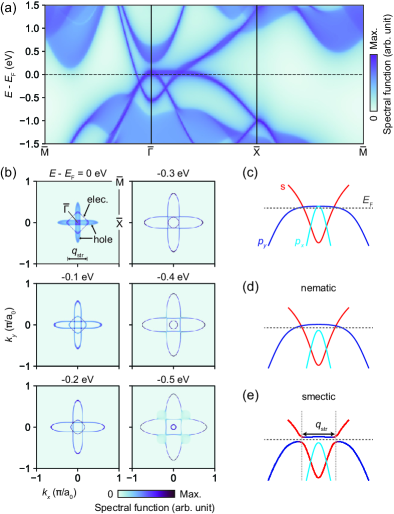
Density Functional Theory (DFT) calculations were performed on NaAlSi using the Vienna Ab initio Simulation Package (VASP) to determine its electronic structure. These calculations employed a plane-wave basis set with an energy cutoff of 400 eV and utilized the Perdew-Burke-Ernzerhof (PBE) generalized gradient approximation for the exchange-correlation functional. Convergence was assessed with respect to both k-point sampling and energy cutoff, ensuring total energies converged to within 1 meV. The electronic structure was then analyzed to characterize the band dispersion, density of states, and identify topological features present in the material.
Wannier function interpolation, applied to Density Functional Theory (DFT) calculations of NaAlSi, facilitates a detailed understanding of its nodal-line semimetal behavior by providing a smooth and accurate representation of the electronic band structure in reciprocal space. This method constructs Wannier functions, which are optimally localized orbitals, and then interpolates between k-points to map out the full band connectivity. Analysis of these interpolated bands reveals the formation of Dirac-like nodal lines protected by the material’s symmetry, specifically occurring at points where conduction and valence bands touch linearly. The resulting band structure confirms that these nodal lines are responsible for the unique electronic properties observed in NaAlSi, enabling high carrier mobility and other characteristics of a topological semimetal.
The crystallographic symmetry of NaAlSi, specifically its classification within the P4/nmm space group, is fundamental to the computational modeling process. This symmetry dictates the arrangement of atoms within the unit cell and consequently influences the selection of appropriate basis sets and k-point sampling schemes within Density Functional Theory (DFT) calculations. Accurate representation of the P4/nmm symmetry reduces the computational demands by allowing the exploitation of symmetry-adapted functions and ensures that calculated electronic properties reflect the material’s true behavior. Deviations from this symmetry in the computational model, even minor ones, can lead to spurious results and inaccurate predictions of the electronic structure.
Density Functional Theory (DFT) calculations have established that the Na-terminated surface of NaAlSi exhibits C4v symmetry. This symmetry dictates the arrangement of atoms and the resulting potential experienced by electrons at the surface. Consequently, the C4v symmetry significantly influences the electronic band structure, leading to specific energy levels and band dispersions. The observed band structure is directly correlated with the surface atomic arrangement dictated by the C4v point group, impacting the material’s electronic properties and potentially its reactivity.
Direct Observation of Charge Modulation
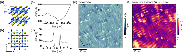
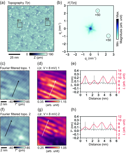
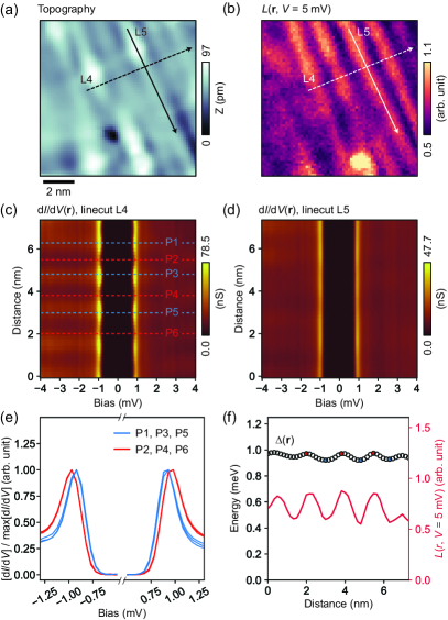
Scanning Tunneling Microscopy (STM) was employed to directly observe the spatial modulation of electronic charge in NaAlSi. This technique relies on a sharp metallic tip brought into close proximity with the sample surface, allowing electrons to tunnel between the tip and the material. Variations in the tunneling current, sensitive to local changes in the electronic density of states, are then mapped to create a topographical image of the charge distribution. In the case of NaAlSi, STM imaging revealed alternating regions of high and low electronic density, indicative of charge stripes forming an ordered pattern at the surface. The atomic-scale resolution of STM enabled direct visualization of these charge stripes, confirming their presence and providing data for subsequent characterization of their periodicity and orientation.
Scanning Tunneling Microscopy (STM) imaging of NaAlSi reveals a charge stripe order characterized by incommensurability with the underlying crystal lattice. This incommensurate behavior indicates that the periodicity of the charge stripes is not a simple rational fraction of the lattice spacing. Specifically, the observed stripe wavelength does not conform to a pattern easily expressed as a ratio of integers related to the lattice parameters. This contrasts with commensurate charge modulations where the stripe periodicity is directly related to the underlying lattice structure through a simple ratio, and necessitates a more complex description of the electronic structure driving the observed charge ordering.
Analysis of the Scanning Tunneling Microscopy (STM) data relied on performing a Fourier transform to convert the real-space images into reciprocal space, where spatial frequencies correspond to the periodicity of the charge stripes. The resulting diffraction pattern exhibited broadened peaks due to imperfections and finite size effects; therefore, peak positions were determined through Lorentzian fitting. The wavelength λ of the charge stripes was then calculated directly from the fitted peak positions in reciprocal space using the relationship \lambda = \frac{1}{q} , where q represents the wavevector corresponding to the charge stripe periodicity. This Lorentzian fitting procedure enabled wavelength determination with a precision significantly exceeding that achievable through direct measurement in real space.
The charge stripe order observed in NaAlSi shares similarities with charge density waves (CDWs) – periodic modulations of electronic density – found in various materials, but exhibits key distinctions. While both involve spatially varying charge distributions, the NaAlSi charge stripes demonstrate a degree of disorder and lack the long-range coherence typically characteristic of CDWs. Furthermore, analysis indicates the driving force behind the NaAlSi ordering is not solely related to Fermi surface nesting – a common mechanism for CDW formation – suggesting a more complex origin potentially involving competing electronic and structural instabilities. This nuanced behavior positions the observed charge modulation as a related, yet fundamentally different, phenomenon compared to conventional CDWs.
Emergence of a Novel Superconducting State
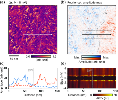
The emergence of a ‘pair liquid crystal’ state arises from the intricate interplay between charge stripe order and superconductivity. In this unique state, the typically isotropic superconducting order parameter-governing the correlated motion of electron pairs-becomes spatially modulated by the periodic potential created by the charge stripes. This modulation doesn’t destroy superconductivity, but rather organizes the Cooper pairs into a nematic-like arrangement, exhibiting directional preferences in their momentum distribution. Essentially, the charge stripes act as a template, inducing a degree of orientational order among the superconducting electrons, leading to a state where superconductivity and liquid crystallinity coexist. This coupling isn’t merely a structural effect; it fundamentally alters the electronic properties, influencing the superconducting gap – measured at 1 meV – and the coherence lengths, which are anisotropic, reaching 9.07 nm perpendicular and 20.33 nm parallel to the stripes.
The emergence of charge stripe order within the superconducting material fundamentally alters the symmetry of the electron pairing. Normally, superconductivity exhibits rotational symmetry, meaning its properties are uniform in all directions; however, the periodic arrangement of charge stripes introduces a preferred direction, effectively breaking this symmetry. This manifests as a liquid crystal-like phase – specifically, either a nematic or smectic phase – within the superconductor. In a nematic phase, the superconducting order parameter aligns along the stripes, creating long-range orientational order, while a smectic phase introduces layering in addition to the orientational order. This transition isn’t a simple loss of superconductivity, but rather a reorganization of the paired electrons into a state where their properties are anisotropic, dependent on direction relative to the charge stripes, and exhibiting a unique interplay between superconducting and structural order.
The emergence of a liquid crystal-like state within the superconductor reveals a profound interplay between the material’s charge density waves and the superconducting electrons. This isn’t a simple coexistence; rather, the superconducting ‘pairs’ align themselves with the periodic modulation of charge, much like molecules in a liquid crystal. This coupling isn’t merely structural, but fundamentally alters the superconducting state, breaking its typical rotational symmetry and creating directional preferences in how the electrons pair and move. Measurements indicate a superconducting gap of 1 meV, and the anisotropic coherence lengths – 9.07 nm perpendicular and 20.33 nm parallel to the charge stripes – directly reflect this intimate connection, demonstrating that the charge density modulation actively sculpts the superconducting order parameter and gives rise to this novel quantum state.
Recent observations reveal a departure from traditional superconductivity, presenting a system where the superconducting energy gap reaches 1 meV at an effective electron temperature of 350 mK. This unconventional behavior is characterized by anisotropic coherence lengths – 9.07 nm perpendicular and 20.33 nm parallel to the charge stripes – determined through detailed Lorentzian fitting of the charge stripe order parameter. The bulk superconducting transition temperature, Tc, is measured at 7.2 K. These parameters collectively suggest a novel interplay between superconductivity and charge density modulation, hinting at the emergence of exotic quantum phases and prompting a re-evaluation of established superconductivity theories. The anisotropic coherence lengths, in particular, signify that superconducting electron pairs are not behaving isotropically, potentially due to the influence of the charge stripe order and opening new avenues for exploring complex quantum phenomena.
The pursuit of novel states of matter often leads to needlessly complex descriptions. This study, detailing the co-existence of electronic smectic phases and superconductivity in NaAlSi, is a welcome corrective. They built a framework of charge stripe order to explain the incommensurate modulation, but the elegance lies in recognizing the underlying connection – the emergence of liquid crystal behavior within a material exhibiting superconductivity. As Jürgen Habermas observed, “The unexamined life is not worth living.” Similarly, the unexamined material – one where emergent properties aren’t linked to fundamental behaviors – offers limited insight. This work, in its clarity, suggests a path towards understanding how collective electronic phenomena can give rise to macroscopic quantum effects.
Where Do We Go From Here?
The observation of smectic order arising from charge density waves in NaAlSi is not, in itself, surprising. What demands further scrutiny is the apparent coupling to superconductivity within a system dominated by pp-orbital interactions. Most investigations in this area have favored s-wave pairing, often mediated by phonons. The emergence of superconductivity in a distinctly anisotropic, charge-ordered state suggests a more complex mechanism, one that necessitates a reassessment of pairing symmetries and mediating interactions in similar materials.
Current density functional theory calculations, while valuable, remain approximations. A complete understanding will require accounting for strong correlation effects and potentially, incorporating many-body techniques. The challenge lies not simply in increasing computational precision, but in identifying the minimal set of parameters necessary to accurately describe the observed phenomena – a ruthless pruning of complexity, if you will.
Future work should prioritize materials exhibiting similar nodal-line semimetallic behavior, but with tunable electronic properties. A systematic investigation of the interplay between charge order, electronic anisotropy, and superconductivity may reveal universal principles governing these correlated electron systems. The ultimate goal, of course, is not merely to catalog observations, but to distill them into a concise and elegant theoretical framework-to find, within the apparent chaos, a signal of underlying order.
Original article: https://arxiv.org/pdf/2601.10939.pdf
Contact the author: https://www.linkedin.com/in/avetisyan/
See also:
- Surprise Isekai Anime Confirms Season 2 With New Crunchyroll Streaming Release
- The Super Mario Galaxy Movie: 50 Easter Eggs, References & Major Cameos Explained
- Starfield (PS5) Review – A Successful Cross-Console Voyage
- HBO Max Just Added the Final Episodes of a Modern Adult Swim Classic
- 10 Best Free Games on Steam in 2026, Ranked
- Sydney Sweeney’s The Housemaid 2 Sets Streaming Release Date
- Preview: Sword Art Online Returns to PS5 as a Darker Open World Action RPG This Summer
- ‘Project Hail Mary’: The Biggest Differences From the Book, Explained
- All 7 New Supes In The Boys Season 5 & Their Powers Explained
- Frieren: Beyond Journey’s End Gets a New Release After Season 2 Finale
2026-01-21 02:38