Author: Denis Avetisyan
A new spectroscopic technique allows researchers to directly map the geometric and topological properties of materials by analyzing how light interacts with their electronic structure.
This review details a method for resolving band topology and quantum geometry via spectroscopic intensities and the wavefunction form factor, revealing key properties like Berry curvature and Wilson loops.
Determining the full quantum geometric and topological properties of electronic bandstructures remains a central challenge in condensed matter physics. In ‘Resolution of Topology and Geometry from Momentum-Resolved Spectroscopies’, we introduce the ‘wavefunction form factor’ (WFF)-a directly measurable quantity derived from momentum- and energy-resolved spectroscopic intensities-to resolve this limitation. This framework reveals topological invariants through ‘spectral nodes’ and provides a model-independent route to quantifying both the non-Abelian Berry curvature and quantum metric. Could this approach unlock a more complete understanding of material properties and pave the way for designing novel quantum materials?
Band Topology: Beyond Simple Energy Levels
Conventional band structure analysis, while foundational in materials science, frequently overlooks critical topological features that profoundly influence a material’s physical properties. These omissions arise because traditional methods primarily focus on the energy levels of electrons within a solid, neglecting the geometric arrangement and phase of the electron wavefunctions. This simplification can mask the existence of topological invariants – mathematical quantities that describe the global properties of the band structure and dictate unusual behaviors like protected surface states and robust electronic transport. Consequently, materials exhibiting fascinating phenomena due to their topology may be mischaracterized or their potential unrealized, highlighting the need for analytical approaches that fully capture the wavefunction geometry beyond simple energy considerations.
Conventional band structure analysis, while focused on the energies of electrons within a material, provides an incomplete picture of its behavior. A full understanding necessitates considering the geometric properties of the electron wavefunctions themselves. These wavefunctions, which describe the probability of finding an electron at a given point, aren’t simply defined by energy; their spatial distribution-how they overlap and interact-holds critical information about the material’s fundamental topological characteristics. Specifically, the geometry of these wavefunctions dictates how electrons move within the material, influencing properties like conductivity and response to external fields. Analyzing this wavefunction geometry allows scientists to identify and characterize topological features within the band structure that are often missed by traditional methods, ultimately providing a more complete and accurate description of the material’s electronic properties.
A comprehensive understanding of a material’s electronic band structure demands more than simply identifying points where bands cross or touch; it requires detailed analysis of the wavefunctions themselves. These wavefunctions, which dictate the probability of finding an electron at a given location, exhibit subtle overlaps that encode crucial geometric information about the band topology. Investigating these wavefunction overlaps reveals how electrons propagate through the material and provides insights into emergent phenomena often missed by traditional band structure analyses. By moving beyond simplistic band crossing models, researchers can unlock a more complete picture of a material’s electronic properties and potentially design materials with tailored functionalities, as the geometry of these wavefunctions directly influences observable physical properties like conductivity and optical response.
The Wavefunction Form Factor (WFF) emerges as a robust tool for characterizing the geometric underpinnings of electronic band structure, offering a pathway to discern topological properties often obscured by traditional analyses. This approach doesn’t merely identify band crossings, but instead quantifies how atomic orbitals hybridize across momentum space, revealing subtle features crucial for understanding material behavior. By directly linking spectroscopic intensities – the brightness observed in experiments like angle-resolved photoemission spectroscopy – to the underlying wavefunction geometry, the WFF allows for the reconstruction of a material’s band topology. This capability represents a significant advancement, as it establishes a direct connection between experimentally accessible data and the abstract mathematical concept of topology, potentially enabling the design of novel materials with tailored electronic properties and robust functionalities.
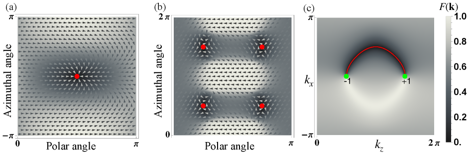
![Calculations of the Wannier function determinant <span class="katex-eq" data-katex-display="false">\det[F(\\mathbf{k})]</span> in <span class="katex-eq" data-katex-display="false">\text{Cu}_{3}\text{TeO}_{6}</span> reveal a spectral node (a) and a nodal arc (b) connecting Dirac points, confirming a non-trivial <span class="katex-eq" data-katex-display="false">Z_{2}</span> charge and its compatibility with the material’s [111] rotation symmetry.](https://arxiv.org/html/2601.10677v1/x3.png)
Mapping Wavefunction Geometry: Tools of the Trade
Angle-Resolved Photoemission Spectroscopy (ARPES) and Inelastic Neutron Scattering are complementary techniques utilized to directly map the electronic band structure of materials. ARPES measures the kinetic energy and momentum of electrons emitted from a sample upon irradiation with photons, providing information about occupied electronic states. Conversely, Inelastic Neutron Scattering probes the energy and momentum transfer of neutrons scattered by the sample, revealing information about both occupied and unoccupied states through the measurement of excitations. The combination of these techniques offers a comprehensive understanding of the material’s electronic structure, including band dispersion, effective mass, and Fermi surface topology, which are crucial for determining material properties and functionalities.
The Wavefunction Form Factor, a critical descriptor of electronic structure, is experimentally accessible through the combined analysis of Angle-Resolved Photoemission Spectroscopy (ARPES) and Inelastic Neutron Scattering data. ARPES directly maps the momentum-dependent spectral function, providing information about the occupied electronic states, while Inelastic Neutron Scattering probes the dynamic charge response. By meticulously analyzing the momentum and energy distributions obtained from these techniques, researchers can reconstruct the Fourier transform of the wavefunction, which defines the Wavefunction Form Factor. This process involves accounting for matrix elements and polarization effects inherent in both spectroscopies to accurately represent the spatial distribution of the electronic wavefunction and quantify its symmetry properties.
The Wavefunction Form Factor (WFF), experimentally determined through techniques like Angle-Resolved Photoemission Spectroscopy (ARPES) and Inelastic Neutron Scattering, directly reflects the spatial distribution of electron wavefunctions within a material. This factor, mathematically representing the Fourier transform of the wavefunction’s probability density, provides a quantitative basis for understanding the wavefunction’s geometry – including its symmetry, nodal structure, and overall shape. By accurately mapping the WFF in reciprocal space, researchers gain critical insight into the real-space wavefunction, enabling the characterization of electronic states and their contribution to material properties. The WFF, therefore, moves beyond simply describing energy and momentum; it provides the geometrical information necessary to fully define the electronic wavefunction and its behavior within the crystal lattice.
The identification of topological features within a material’s band structure relies on mapping the Wavefunction Form Factor, a process requiring a minimum of N_p probes. This probe number must be equal to or exceed the rank of the band projector, denoted as N_b . The rank N_b defines the number of independent wavefunctions contributing to a given band, and therefore, to accurately characterize the wavefunction geometry and identify topological invariants, the number of probes N_p used to map the Wavefunction Form Factor must satisfy the condition N_p \geq N_b . Insufficient probing can lead to an incomplete or inaccurate representation of the wavefunction, obscuring crucial topological information.
Decoding Topology: Signatures in the Form Factor
The Wavefunction Form Factor (WFF), a determinant constructed from the wavefunction of a system, is mathematically constrained by the Topological Selection Rule. This rule dictates that nontrivial topological phases necessitate the presence of zeros within the WFF determinant, referred to as Spectral Nodes. The location and degree of these nodes are not arbitrary; they are directly linked to the topological charge of the system. Specifically, each Spectral Node contributes to the overall topological charge, and the sum of the degrees of all nodes provides a quantitative measure – ∑d(ki) = total charge mod 2 for Z2 topological indices – verifying the consistency between the WFF analysis and established topological invariants.
Spectral nodes, arising as zeros in the Wavefunction Form Factor determinant, function as reliable indicators of nontrivial band topology. Their robustness stems from being protected by the underlying symmetries of the system, meaning they are less susceptible to perturbations that might alter other band structure features. The presence of these nodes directly correlates with topological invariants; specifically, the degree of each node contributes to the overall topological charge of the material. Consequently, analyzing the number and degree of spectral nodes provides a direct method for identifying and characterizing topological states of matter without requiring a full band structure calculation or knowledge of the system’s symmetry group, offering a computationally efficient means of topological material discovery.
The Wavefunction Form Factor, beyond identifying Spectral Nodes, facilitates the construction of an Effective Band Projector. This projector, derived from the Form Factor, provides a real-space representation of the band structure’s topological properties. Specifically, it allows for the direct visualization of edge states and their correspondence to bulk band topology. By projecting the Hamiltonian onto the subspace defined by the Wavefunction Form Factor, researchers can isolate and analyze the topological features of the band structure, offering a complementary method to traditional band structure calculations and providing a more intuitive understanding of topological states.
The topological selection rule provides a quantifiable link between the wavefunction form factor and topological invariants. Specifically, the total topological charge of a system can be calculated by summing the degrees d(k_i) of all spectral nodes k_i present in the determinant. This summation, represented as ∑d(k_i) = \text{total charge}, yields the full topological charge. For systems exhibiting Z2 topological indices, the result of this summation is taken modulo 2, ensuring the final charge is an integer value reflecting the topological classification.
From Topology to Function: The Promise of New Physics
The Quantum Geometric Tensor represents a fundamental shift in how materials respond to external influences, moving beyond traditional descriptions of symmetry and electronic band structure. This tensor isn’t a single entity, but rather a combination of two key components: Berry Curvature and the Quantum Metric. Berry Curvature describes how the wave function of an electron changes as it moves through momentum space, influencing its dynamics and giving rise to phenomena like the anomalous Hall effect. Simultaneously, the Quantum Metric dictates the intrinsic geometry of the momentum space itself, governing the velocity of electrons and their susceptibility to external fields. Together, these components create a comprehensive picture of a material’s response, allowing researchers to predict and potentially control its behavior under stress, electric fields, or light exposure – unlocking possibilities for novel electronic devices and materials with tailored properties. The tensor’s ability to capture both the curvature and the inherent shape of momentum space provides a powerful tool for understanding complex material behavior beyond simple band theory.
The quantum metric, a fundamental component of the quantum geometric tensor, dictates the behavior of electrons in materials exhibiting flat band dispersion – a condition where electrons possess zero kinetic energy. This seemingly unusual state has profound consequences for a material’s optical properties, directly influencing its response to light. Specifically, the quantum metric determines the strength of nonlinear optical effects, enabling phenomena such as second harmonic generation and efficient frequency mixing. Materials with large quantum metrics can therefore dramatically enhance these interactions, potentially leading to the development of novel photonic devices and technologies. Understanding and engineering the quantum metric offers a pathway to control light-matter interactions at a fundamental level, promising advancements in areas like optical computing and sensing. The magnitude of these effects is directly tied to the ‘flatness’ of the band, with perfectly flat bands theoretically exhibiting infinite nonlinear responses.
The classification of matter hinges on identifying properties that remain constant despite continuous deformations – a cornerstone of topology. Scientists utilize topological invariants, such as the Chern number and the Z2 index, to categorize distinct phases of matter beyond traditional order parameters. These invariants are global properties of the electronic band structure, effectively acting as ‘fingerprints’ for different quantum states. A non-zero Chern number, for example, signals the existence of chiral edge states, robust to backscattering and crucial for dissipationless transport. Similarly, the Z2 index distinguishes between topologically trivial and non-trivial insulators. Crucially, predicting these invariants allows researchers to anticipate the emergence of exotic states – including those hosting protected boundary modes or fractionalized excitations – opening avenues for designing materials with unprecedented functionalities and potentially revolutionizing fields like quantum computing and energy storage.
The emerging framework of quantum geometry offers a promising route toward realizing and controlling materials hosting fractionalized excitations, a hallmark of exotic quantum phases like Fractional Chern Insulators. These insulators, distinct from conventional materials, exhibit quasiparticles with fractional electric charge and statistics, arising from the intricate interplay of topology and strong electron correlations. Unlike conventional materials where electrons behave as individual, integer-charged particles, these systems demonstrate collective behavior where electron identity effectively ‘fragments’. This fragmentation isn’t a physical breaking apart of electrons, but rather a manifestation of emergent degrees of freedom governed by the material’s topological properties and the quantum metric – essentially, the way the material responds to changes in its internal geometry. The ability to design materials with specific topological invariants and tailored quantum metrics presents an unprecedented opportunity to not only observe these fascinating fractionalized states but also to harness their unique properties for advanced technological applications, potentially revolutionizing fields like quantum computation and materials science.
The pursuit of neatly classifying band topology, as this paper attempts with spectroscopic intensities and the ‘wavefunction form factor’, feels… familiar. It’s a temporary reprieve from the inevitable chaos. One can meticulously define invariants and geometric properties, but production will always find a way to introduce a material with a confounding defect, a spurious interaction, or a measurement error. As Karl Popper observed, “The only way to guard oneself against the corrupting influence of power is to increase and disperse it.” Similarly, the only way to guard against the corrupting influence of elegant theory is to subject it to relentless, messy data. They’ll call it material characterization and raise funding, but it’s just delaying the tech debt. The documentation always lies, eventually.
What’s Next?
The notion of extracting topological invariants and geometric properties from spectroscopic intensities, via this ‘wavefunction form factor’, feels…familiar. It’s a predictable refinement, really. Someone will inevitably discover that perfectly crystalline samples – the unspoken assumption underpinning these calculations – rarely survive contact with reality. Expect a flurry of papers attempting to account for disorder, defects, and the inevitable surface states. The elegant simplicity will erode, of course, replaced by fitting parameters and ad-hoc corrections. It always does.
One can foresee extensions towards more complex materials, naturally. But the real challenge won’t be scaling to higher dimensions or stranger symmetries. It will be disentangling the contributions of genuine topological features from the mundane effects of band hybridization and electron correlation. The signal, one suspects, will become increasingly buried beneath layers of complexity, requiring ever more sophisticated data analysis – and, ultimately, more assumptions.
Ultimately, this feels less like a revolution and more like a clever repackaging of existing concepts. The method promises a more direct route to characterizing band topology, but it sidesteps the underlying difficulties of actually understanding those bands. It’s a useful tool, certainly, but one should not mistake the map for the territory. Everything new is just the old thing with worse docs.
Original article: https://arxiv.org/pdf/2601.10677.pdf
Contact the author: https://www.linkedin.com/in/avetisyan/
See also:
- Best Controller Settings for ARC Raiders
- The Boys Season 5 Officially Ends An Era For Jensen Ackles’ Soldier Boy
- Review: Final Fantasy Tactics: The Ivalice Chronicles (PS5) – Still the Benchmark for Turn-Based Tactics
- Nippon Sangoku Is The Best New Post-Apocalyptic Anime of Spring 2026
- Mark Zuckerberg & Wife Priscilla Chan Make Surprise Debut at Met Gala
- Elon Musk’s Mom Maye Musk Shares Her Parenting Philosophy
- 10 Greatest Manga Endings of All Time
- The Witcher 3 Officially Reveals Stunning New Ciri Figure Coming 2026
- The WONDERfools ending explained: What happened to the Child of Eternity?
- 7 Great Marvel Villains Who Are Currently Dead
2026-01-16 11:30